
Semiconductor Light Emitting Device and Multiple Lead Frame for Semiconductor Light Emitting Device

a light-emitting device and semiconductor technology, applied in the direction of electrical apparatus construction details, casings/cabinets/drawers, electrical apparatus details, etc., can solve the problems of difficult clamping of dies, difficult to ensure uniform sealing shape, and inability to control optical characteristics by the shape of resin sealing, etc., to achieve excellent heat radiation and easy application

Active Publication Date: 2008-09-18
XIAMEN SANAN OPTOELECTRONICS CO LTD
View PDF15 Cites 83 Cited by
  • Summary
  • Abstract
  • Description
  • Claims
  • Application Information

AI Technical Summary

Benefits of technology

[0012]The primary object of the present invention is to provide a semiconductor light emitting device and a multiple lead frame for a semiconductor light emitting device, which are excellent in heat radiation and which is easily applied to die molding for ensuring the sealing shape having intended optical characteristics.

Problems solved by technology

However, according to this method, the shape of epoxy resin 106 is limited to the shape of the concave shape formed by resin portion 103, and the optical characteristics by the shape of resin sealing cannot be controlled.
Therefore, it is difficult to ensure uniform sealing shape.
However, as resin portion 103 is protruding on main surface 101a of lead frame 101, clamping of the die is difficult.
However, sealing only the periphery of LED chip 104 with epoxy resin 106 is difficult because of the limited clamping region and in consideration of keeping the region for resin gate and runner.
Also, there is a disadvantage that it is easily damaged when clamped by the die.
This insulating layer reduces the thermal conductivity.

Method used


Image

  • Semiconductor Light Emitting Device and Multiple Lead Frame for Semiconductor Light Emitting Device
  • Semiconductor Light Emitting Device and Multiple Lead Frame for Semiconductor Light Emitting Device
  • Semiconductor Light Emitting Device and Multiple Lead Frame for Semiconductor Light Emitting Device

Examples


first embodiment

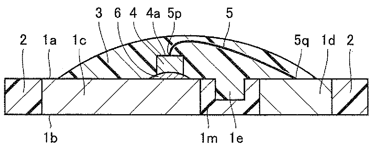
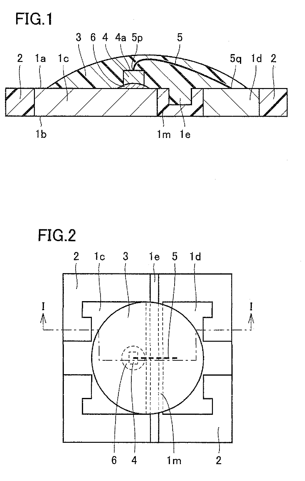
[0057]As shown in FIGS. 1 and 2, a semiconductor light emitting device includes a lead frame 1 having a main surface 1a, a resin portion 2 as an insulator provided so as to surround lead frame 1 and to have the thickness not greater than that of lead frame 1, an LED chip 4 as a semiconductor light emitting element provided on main surface 1a, a metal wire 5, and a thermosetting resin 3 as a sealing resin provided so as to completely cover LED chip 4 and metal wire 5.

[0058]Lead frame 1 includes a semiconductor light emitting element mounting portion 1c having LED chip 4 mounted on main surface 1a. Lead frame 1 also includes a metal wire connecting portion 1d that is electrically connected to LED chip 4 by metal wire 5 and that extends over the same plane as semiconductor light emitting element mounting portion 1c. Semiconductor light emitting element mounting portion 1c and metal wire connecting portion 1d are surrounded by resin portion 2. Resin portion 2 forms the outer shape of th...

second embodiment

[0091]As shown in FIG. 6, a semiconductor light emitting device of a second embodiment is different from the semiconductor light emitting device of the first embodiment shown in FIG. 1 in the shape of thermosetting resin 3 as a sealing resin and the shape of the resin arranged inside slit-like groove 1m.

[0092]Specifically, thermosetting resin 3 is molded into a cylindrical shape. In the second embodiment, thermosetting resin 3 is molded by dam-sheet molding. On the surface, on main surface 1a side, of the resin arranged inside slit-like groove 1m, depression 1e for runner and air vent of injection molding is not formed.

[0093]As used herein, the dam-sheet molding refers to a method of molding thermosetting resin, wherein a sheet made of silicone, Teflon (registered trademark) or the like having a hole (a dam sheet) is attached to a lead frame, into which hole resin is poured by potting method. In this state, the resin is thermally cured. Thereafter, the dam sheet is peeled off to le...

third embodiment

[0097]As shown in FIGS. 7 and 8, a semiconductor light emitting device of a third embodiment is different from the semiconductor light emitting device of the first embodiment shown in FIGS. 1 and 2 in the shape of main surface 1a of lead frame 1.

[0098]Specifically, on main surface 1a, concave portion 8 is formed over semiconductor light emitting element mounting portion 1e, slit-like groove 1m, and metal wire connecting portion 1d. LED chip 4 as a semiconductor light emitting element is mounted on semiconductor light emitting element mounting portion 1c with silver paste 6 interposed, at bottom surface 5a of concave portion 8. To bottom portion 5a of concave portion 8 in metal wire connecting portion 1d, metal wire 5 extending from the top surface of LED chip 4 is connected. The side wall of concave portion 8 is formed to be tilted such that the opening area of concave portion 8 on the same plane as main surface 1a is greater than the area of bottom surface 5a of concave portion 8.

[...


PUM


Abstract

A semiconductor light emitting device that is excellent in radiating heat and that can be molded into a sealing shape having intended optical characteristics by die molding is provided. The semiconductor light emitting device includes: a lead frame including a plate-like semiconductor light emitting element mounting portion having an LED chip mounted on a main surface, and a plate-like metal wire connecting portion extending over a same plane as the semiconductor light emitting element mounting portion; a metal wire electrically connecting the LED chip and the metal wire connecting portion; a thermosetting resin molded by die molding or dam-sheet molding so as to completely cover the LED chip and the metal wire; and a resin portion provided to surround the lead frame and having the thickness not greater than the thickness of the lead frame.

Description

[0001]This nonprovisional application is based on Japanese Patent Application No. 2007-063698 filed with the Japan Patent Office on Mar. 13, 2007, the entire contents of which are hereby incorporated by reference.BACKGROUND OF THE INVENTION[0002]1. Field of the Invention[0003]The present invention relates to a semiconductor light emitting device on which a semiconductor light emitting element is mounted, and a multiple lead frame for a semiconductor light emitting device.[0004]2. Description of the Background Art[0005]Conventional semiconductor light emitting devices are disclosed in, for example, Japanese Patent Laying-Open Nos. 2004-274027, 07-235696 and 2002-141558. As shown in FIG. 21, a conventional semiconductor light emitting device includes a lead frame 101 having a main surface 101a, an LED (Light Emitting Diode) chip 104 provided on main surface 101a, a metal wire 105 connecting lead frame 101 and LED chip 104, epoxy resin 106 provided on main surface 101a so as to complet...

Claims


Application Information

Patent Timeline
IPC IPC(8): H01L33/00H05K7/18H01L33/56H01L33/60H01L33/62H01L33/64
CPCH01L33/486H01L33/52H01L2924/12041H01L33/62H01L2224/97H01L2224/32257H01L2924/3025H01L2224/73265H01L2224/48247H01L2224/32245H01L24/97H01L2224/45144H01L2924/01019H01L2924/3011H01L2924/01079H01L2924/01078H01L2924/01046H01L2924/01012H01L2224/48091H01L33/647H01L33/54H01L33/60H01L33/641H01L2924/00014H01L2924/00H01L2224/85H01L2924/15787H01L2924/181H01L2924/12042H01L2924/00012
Inventor TAKADA, TOSHIYUKI
Owner XIAMEN SANAN OPTOELECTRONICS CO LTD
Features
  • Generate Ideas
  • Intellectual Property
  • Life Sciences
  • Materials
  • Tech Scout
  • Unparalleled Data Quality
  • Higher Quality Content
  • 60% Fewer Hallucinations
Learn More