This helps you quickly interpret patents by identifying the three key elements:
Problems solved by technology
Method used
Benefits of technology
Benefits of technology
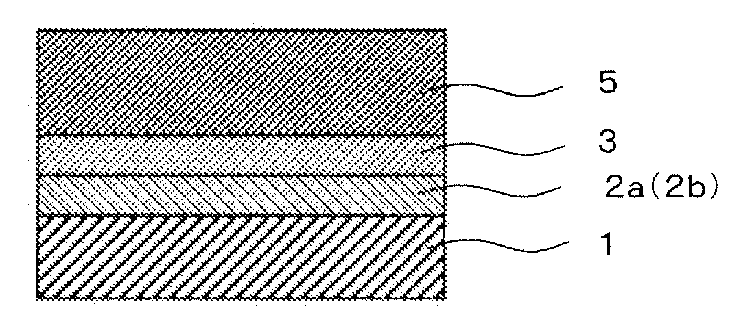
[0025]Moreover, the formation of the GaN and AlN superlattice structure more improves the crystallinity of the nitride semiconductor single crystal film.
[0026]Therefore, the nitride semiconductor single crystal substrate maybe used suitably for light-emitting diode
Problems solved by technology
Because the above nitride semiconductors have a high melting point and the equilibrium vapor pressure of nitrogen is very high, the growth of a bulk crystal from a molten solution is not easy.
However, when a nitride semiconductor single crystal film is formed, a Si substrate being used, the nitride semiconductor single crystal film is broken because of a difference in thermal expansion coefficient between Si and a nitride semiconductor, and also, many crystal defects are caused by a difference in crystal lattice constant between Si
Method used
Image
Click on the blue label to locate the original text in one second.
Reading with bidirectional positioning of images and text.
Examples
Example
Example 1
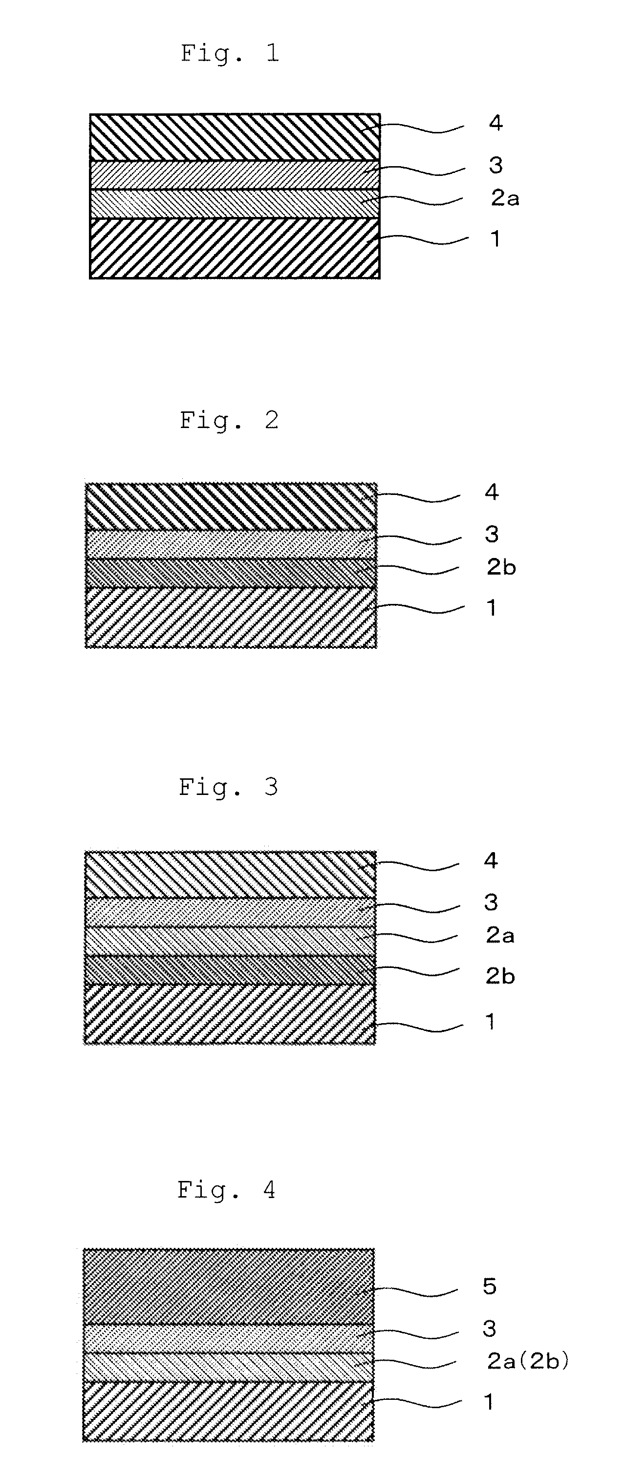
[0059]A Si substrate made of Si (100) off-cut at an angle of 8° in the direction from the direction was set to the growth zone in a reaction tube and the above Si substrate was heated to 1100° C. with supplying hydrogen as a carrier gas to carry out cleaning of the surface of the substrate.
[0060]Then, propane was supplied and the temperature of the substrate was set to 1000 to 1350° C. to carbonize the surface of the Si substrate. Then, propane and silane were supplied to form a SiC buffer layer of 10 to 10000 nm in thickness.
[0061]Next, trimethylalminium (TMA) and ammonia were supplied as raw materials while keeping the temperature of the substrate to form an AlN buffer layer of 1 to 500 nm in thickness on the above SiC layer.
[0062]Moreover, the temperature of the substrate was dropped to about 1000° C. and trimethylgallium (TMG) and ammonia were supplied as raw materials to form a GaN single crystal film on the above AlN buffer layer.
[0063]Even when the above GaN singl...
Example
Example 2
[0064]A SiC buffer layer and an AlN buffer layer were formed on a Si substrate made of Si (100) off-cut at an angle of 8° in the direction from the direction in the same manner as in Example 1.
[0065]Next, the substrate was heated to 1200° C. or more and TMA and ammonia were supplied as raw materials to form an AlN single crystal film on the above AlN buffer layer.
[0066]Even when the above AlN single crystal film was formed in a thickness of 1 μm or more, a flat surface was obtained without any cracks found thereon. Also, the azimuth of the orientation was .
Example
Example 3
[0067]A SiC buffer layer and an AlN buffer layer were formed on a Si substrate made of Si (100) off-cut at an angle of 8° in the direction from the direction in the same manner as in Example 1.
[0068]Next, the substrate was heated to 500° C. or more and trimethylindium (TMIn) and ammonia were supplied as raw materials to form an InN single crystal film on the above AlN buffer layer.
[0069]Even when the above InN single crystal film was formed in a thickness of 1 μm or more, a flat surface was obtained without any cracks found thereon. Also, the azimuth of the orientation was .
PUM
Abstract
To provide a nitride semiconductor single crystal substrate comprising a Si substrate and a nitride semiconductor film which has semi-polar (10-1m) plane (m: natural number) and a thickness of 1 μm or more, the nitride semiconductor single crystal substrate being suitably used for a light-emitting device, the nitride semiconductor single crystal substrate being suitably used for a light-emitting device, this invention provides a nitride semiconductor single crystal substrate comprising a Si substrate having an off-cut angle of 1 to 35° in the <110> direction from the <100> direction, a buffer layer 2a (2b) made of at least one of SiC or BP formed on the Si substrate, a AlN buffer layer formed on the buffer layers, and a nitride semiconductor single crystal film formed on the AlN buffer layer, the nitride semiconductor single crystal film comprising any one of GaN (10-1m), AlN (10-1m), InN (10-1m) or a GaN (10-1m)/and AlN (10-1m) superlattice film.
Description
BACKGROUND OF THE INVENTION[0001]1. Field of the Invention[0002]The present invention relates to a nitride semiconductor single crystal made of gallium nitride (GaN), aluminum nitride (AlN) and the like to be used suitably for light-emitting diodes, laser light-emitting diodes, high-speed and high-temperature operable electronic elements.[0003]2. Description of the Related Art[0004]Nitride semiconductors typified by GaN and AlN have a wide band gap and are materials expected to be applied to light-emitting diodes, laser light-emitting elements or high-speed and high-temperature operable electronic elements or the like as compound semiconductors having excellent characteristics such as high electron mobility and high heat resistance.[0005]Because the above nitride semiconductors have a high melting point and the equilibrium vapor pressure of nitrogen is very high, the growth of a bulk crystal from a molten solution is not easy. For this reason, a single crystal of the nitride semicon...
Claims
Application Information
Patent Timeline
Application Date:The date an application was filed.
Publication Date:The date a patent or application was officially published.
First Publication Date:The earliest publication date of a patent with the same application number.
Issue Date:Publication date of the patent grant document.
PCT Entry Date:The Entry date of PCT National Phase.
Estimated Expiry Date:The statutory expiry date of a patent right according to the Patent Law, and it is the longest term of protection that the patent right can achieve without the termination of the patent right due to other reasons(Term extension factor has been taken into account ).
Invalid Date:Actual expiry date is based on effective date or publication date of legal transaction data of invalid patent.

