Flash memory device with reduced coupling effect among cells and method of driving the same

a flash memory and cell technology, applied in static storage, digital storage, instruments, etc., can solve the problems of reducing affecting the reliability of data reads, and not flash memory has a large current consumption, so as to minimize the coupling effect and improve the reliability of reading data.

Active Publication Date: 2008-09-18
SAMSUNG ELECTRONICS CO LTD
View PDF2 Cites 102 Cited by
  • Summary
  • Abstract
  • Description
  • Claims
  • Application Information

AI Technical Summary

Benefits of technology

[0020]The present invention provides a flash memory device that can improve the reliability of re

Problems solved by technology

Conventionally, the NOR flash memory has a large current consumption, and thus, is disadvantageous in terms of high integration.
The co

Method used


Image

  • Flash memory device with reduced coupling effect among cells and method of driving the same
  • Flash memory device with reduced coupling effect among cells and method of driving the same
  • Flash memory device with reduced coupling effect among cells and method of driving the same

Examples


Embodiment Construction

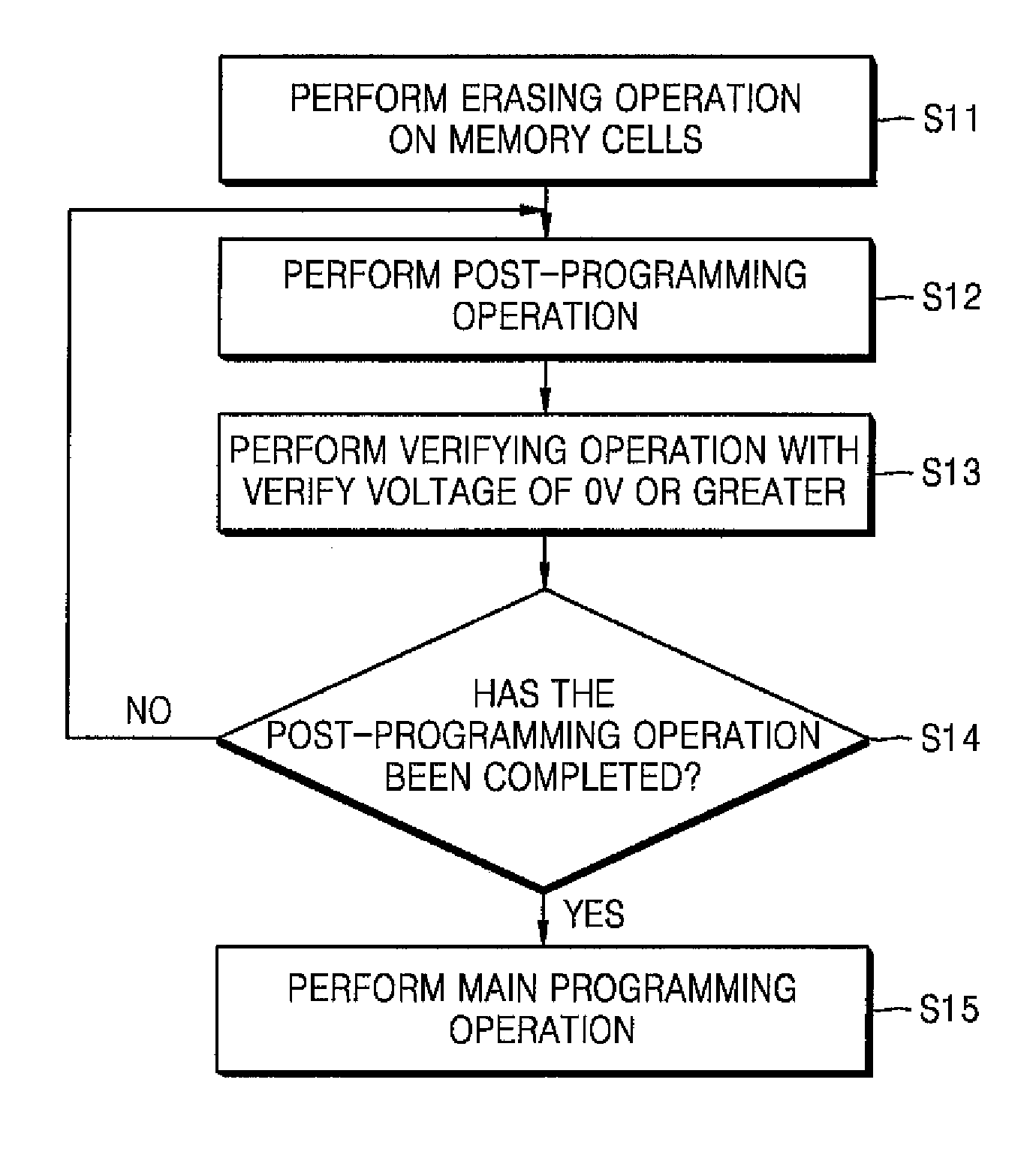
[0036]Hereinafter, the invention will be described in detail by explaining exemplary embodiments of the invention with reference to the attached drawings. Like reference numerals in the drawings denote like elements.

[0037]FIG. 4 is a block diagram of a flash memory device 100 according to an embodiment of the invention. Referring to FIG. 4, the flash memory device 100 may include a memory cell array 110, and a peripheral circuit 120 configured to perform a programming operation or a read operation on the memory cell array 110. The peripheral circuit 120 may include a pre-charging unit 121, a sense amplifying unit 122, an input / output buffer 123, and a write driver 124.

[0038]In addition, the flash memory device 100 includes a control logic 130 configured to control the programming operation or read operation of the memory cell array 110. The flash memory device 100 also includes a pass and fail detecting unit 140 configured to determine whether each memory cell on which the programmi...


PUM


Abstract

Embodiments of the invention provide a flash memory device that can improve the reliability of a reading operation by minimizing a variation in the threshold voltage distribution that occurs due to coupling between cells, and a method of driving the flash memory device. In an embodiment of the invention, the method of driving the flash memory includes: performing an erasing operation on memory cells; after the performing the erasing operation, performing a post-programming operation to control a threshold voltage of the memory cells; and after performing the post-programming operation, performing a main programming operation on the memory cells, wherein the performing of the post-programming operation comprises increasing the threshold voltage of the memory cells in an erased state, thereby reducing a difference in the threshold voltage between the memory cells in the erased state and the memory cells in the programmed state.

Description

CROSS-REFERENCE TO RELATED PATENT APPLICATIONS[0001]This application claims the benefit of Korean Patent Application No. 10-2007-0025630, filed on Mar. 15, 2007, in the Korean Intellectual Property Office, the disclosure of which is incorporated herein in its entirety by reference.BACKGROUND OF THE INVENTION[0002]1. Field of the Invention[0003]The invention relates generally to a flash memory device and a method of driving the same, and more particularly, but without limitation, to a flash memory device that can minimize a variation in a threshold voltage distribution caused by coupling between cells, and a method of driving the same.[0004]2. Description of the Related Art[0005]Flash memories, which are widely used nonvolatile memory devices, can electrically erase or rewrite data. As compared to magnetic disk storage media such as a hard disc, a flash memory has lower power consumption and a shorter access time.[0006]A flash memory is classified as a NOR flash memory or a NAND flas...

Claims


Application Information

Patent Timeline
IPC IPC(8): G11C16/10G11C16/34
CPCG11C11/5628G11C11/5635G11C2211/5621G11C16/3445G11C16/3404G11C16/10G11C16/16G11C16/34
Inventor CHAE, DONG-HYUK
Owner SAMSUNG ELECTRONICS CO LTD
Why Eureka
Try Eureka