Printed circuit board, design method thereof and mainboard of terminal product

a technology of printed circuit board and terminal product, which is applied in the direction of printed circuit aspects, cross-talk/noise/interference reduction, instruments, etc., can solve the problems of increasing the cost of the mainboard pcb, the risk of short supply of existing six-layer hdi boards, and the constant lowering of the hardware cost of the pcb, etc., to achieve convenient adjustment, superior in price, and free of the risk of short supply

Active Publication Date: 2008-09-25
HUAWEI TECH CO LTD
View PDF25 Cites 38 Cited by
  • Summary
  • Abstract
  • Description
  • Claims
  • Application Information

AI Technical Summary

Benefits of technology

[0021]The total board thickness of the inventive four-layer printed circuit board can be adjusted conveniently by changing the thickness of the laminate. The laminates are conventional board materials applied widely and are free of the risk of a short supply. Two laminates are used for the board with mechanical blind vias, and therefore under the precondition of ensuring the flatness of a board and based on the current technologic level, the thinnest fabricable laminate has a thickness of 0.2 mm / 0.3 mm in the practical process, and a controllable board thickness is 0.7 mm / 0.9 mm, which is slightly below a conventional board thickness of the six-layer one-level HDI board. This is suitable for a design of a thin-type device with a special requirement on the strength of a board. As the technologic capabilities of manufacturers advance, the whole board can also become thinner while keeping superior in price to the six-layer board.

Problems solved by technology

As the integration level of devices is improved increasingly, a hardware cost of the PCB is lowered continuously.
The cost of the mainboard PCB is an increasing proportion of the hardware cost of a whole machine, and the signal quality in the PCB also has a direct influence on the performance of the whole device.
However, the existing six-layer HDI board has a relatively high cost due to excessive fabrication processes, a long process cycle and numerous board material layers.
Further, the six-layer HDI board can not be easily made thin in shape due to the fact that the insulation strength between every two of the numerous layers shall be guaranteed necessarily, and that a dielectric layer between respective signal layers shall not be too thin because a too thin inner dielectric layer may result in a lowered qualified rate directly.

Method used


Image

  • Printed circuit board, design method thereof and mainboard of terminal product
  • Printed circuit board, design method thereof and mainboard of terminal product
  • Printed circuit board, design method thereof and mainboard of terminal product

Examples


first embodiment

THE FIRST EMBODIMENT

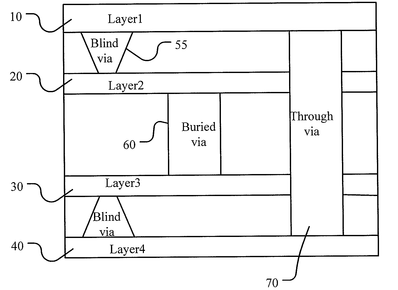
[0046]With reference to FIG. 5, a four-layer HDI board with laser blind vias designed according to the embodiment of the invention includes two outer surface layers, i.e., the first layer (layer 1) 10 and the fourth layer (layer 4) 40, and two inner layers, i.e., the second layer (layer 2) 20 and the third layer (layer 3) 30, and further includes a laser blind via 55, a buried via 60 and a through via 70. The structure illustrated in FIG. 5 is merely illustrative of one of the structure forms according to the embodiment of the invention. FIGS. 6 to 11 schematically illustrates more structure forms of the four-layer printed circuit board with laser blind vias. Specific technical details will be explained below in connection with this preferred embodiment.

[0047]Specific parameters for a design of laminated layers of the four-layer HDI board with laser blind vias are illustrated in Table 1 below.

TABLE 1Board thickness: variableTolerance: + / −0.1 mmReference laminated...

second embodiment

THE SECOND EMBODIMENT

[0133]With reference to FIG. 12, a four-layer PCB board with mechanical blind vias designed according to the embodiment of the invention includes: two surface layers, i.e., the first layer (layer 1) 10 and the fourth layer (layer 4) 40; and two inner layers, i.e., the second layer (layer 2) 20 and the third layer (layer 3) 30. The four-layer PCB board further includes a blind via 50 and a through via 70. The structure illustrated in the FIG. 12 is merely illustrative of one of structure forms of a four-layer PCB board with mechanical blind vias in the embodiment of the invention, and further structure forms of the four-layer PCB board with mechanical blind vias are shown in FIGS. 13-15.

[0134]Special technical details of the four-layer PCB board with mechanical blind vias will be explained below in connection with the preferred embodiment. The embodiment of the four-layer HDI board with laser blind vias can be made reference to for other technical details.

[0135]1...


PUM


Abstract

A printed circuit board and a design method thereof are disclosed. The design method includes: wiring signal lines on an area basis at inner layers adjacent to outer surface layers; arranging the outer surface layers with no wiring or few wirings and interconnecting the outer surface layers by way of through vias, so that the outer surface layers function as a primary ground; and setting parameters of a line width and a layer height to control a target impedance value. The printed circuit board includes outer surface layers and two inner layers therebetween. The inner layers adjacent to the outer surface layers are used for arranging signal lines on an area basis; and the outer surface layers are arranged with no wiring or few wirings and are interconnected as a primary ground through vias. The invention also discloses a mainboard of a terminal product using the printed circuit board.

Description

CROSS-REFERENCE TO RELATED APPLICATIONS[0001]This application claims benefits to Chinese Patent Application No. 200710090909.0, entitled “Printed Circuit Board and Design Method Thereof” and filed on Mar. 23, 2006, and Chinese Patent Application No. 200710127769.X, entitled “Printed Circuit Board, Design Method Thereof and Mainboard of Terminal Product” and filed on Jun. 28, 2007, both of which are incorporated herein by reference in their entireties.FIELD OF THE INVENTION[0002]The present invention relates to Printed Circuit Board (PCB) technologies, and particularly to a multi-layer printed circuit board and a design method thereof. The invention also relates to a mainboard of a terminal product using such printed circuit board.BACKGROUND OF THE INVENTION[0003]A printed circuit board is a structural element formed of insulated materials together with conductor wirings, and is applied to various communication and electronic devices. Printed Circuit Board technologies have been deve...

Claims


Application Information

Patent Timeline
Patent Type & Authority Applications(United States)
IPC IPC(8): H05K1/09G06F17/50
CPCH05K1/0218H05K1/025H05K1/0298H05K2201/0191H05K1/116H05K2201/09536H05K2201/09627G06F1/16H05K1/115H05K2201/0715H05K3/46
Inventor SHEN, XIAOLANYE, QINGSONGWEI, KONGGANG
Owner HUAWEI TECH CO LTD
Why Eureka
Try Eureka