Gas flow diffuser

a technology of gas flow and diffuser, which is applied in the direction of mechanical equipment, branching pipes, transportation and packaging, etc., can solve the problems of loss of etch uniformity, non-uniformity of etch rate across the substrate, and complex devices of integrated circuits

Inactive Publication Date: 2008-09-25
APPLIED MATERIALS INC
View PDF15 Cites 37 Cited by
  • Summary
  • Abstract
  • Description
  • Claims
  • Application Information

AI Technical Summary

Problems solved by technology

Integrated circuits have evolved into complex devices that can include millions of components (e.g., transistors, capacitors, resistors, and the like) on a single chip.
One problem associated with a conventional plasma etch process used in the manufacture of integrated circuits is the non-uniformity of the etch rate across the substrate, which may be due, in part, to a lateral offset between the reactive species and the substrate being etched.
This offset contributes to a loss of etch uniformity over the surface of the substrate which may significantly affect performance and increase the cost of fabricating integrated circuits.
Although this technique has demonstrated good processing results, a level of process uniformity has not been achieved that will enable next generation devices, believed at least in part to be due to the inability to completely compensate for conductance non-uniformity above the substrate being processed within the processing chamber.

Method used


Image

  • Gas flow diffuser
  • Gas flow diffuser
  • Gas flow diffuser

Examples


Embodiment Construction

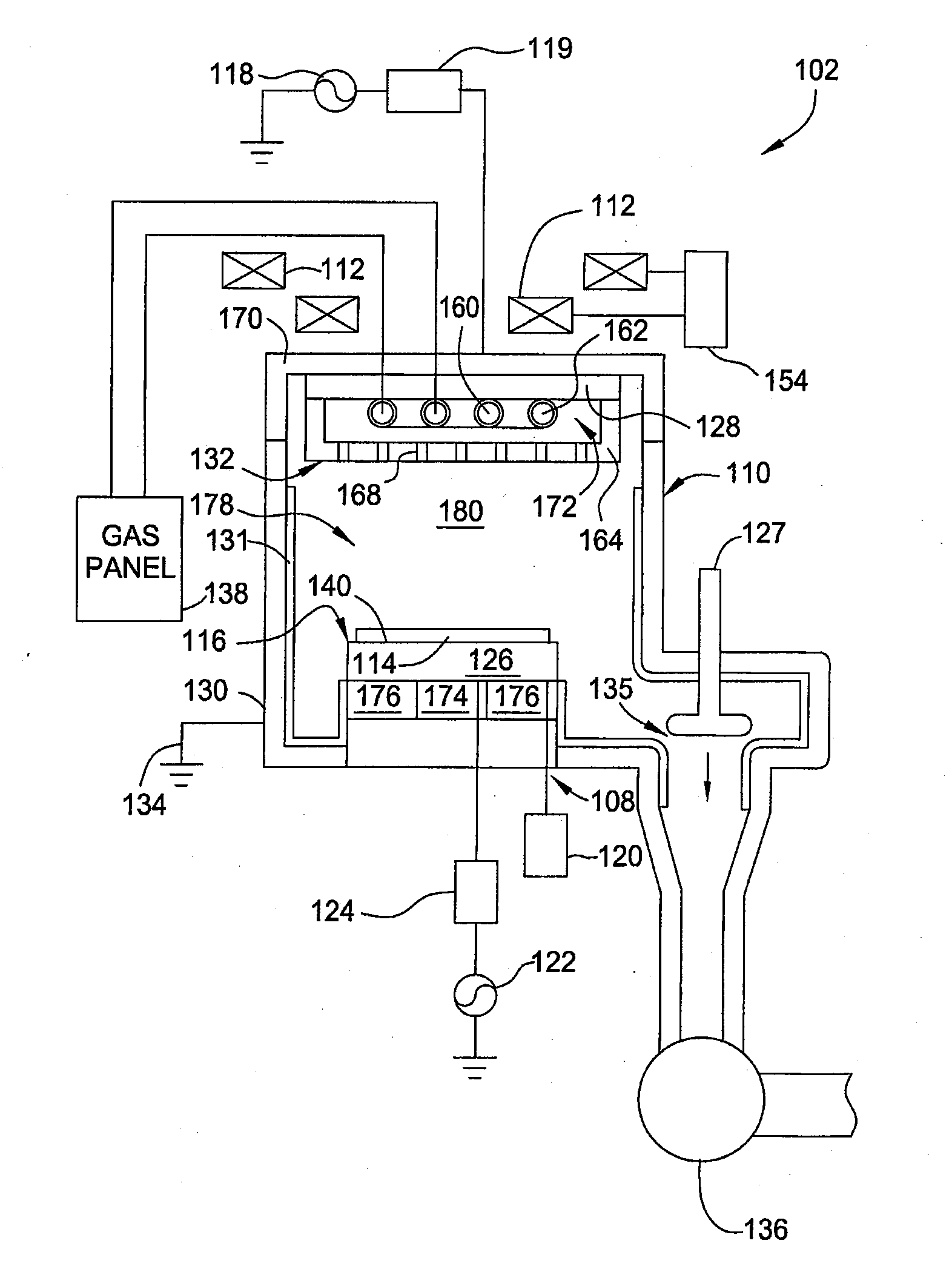
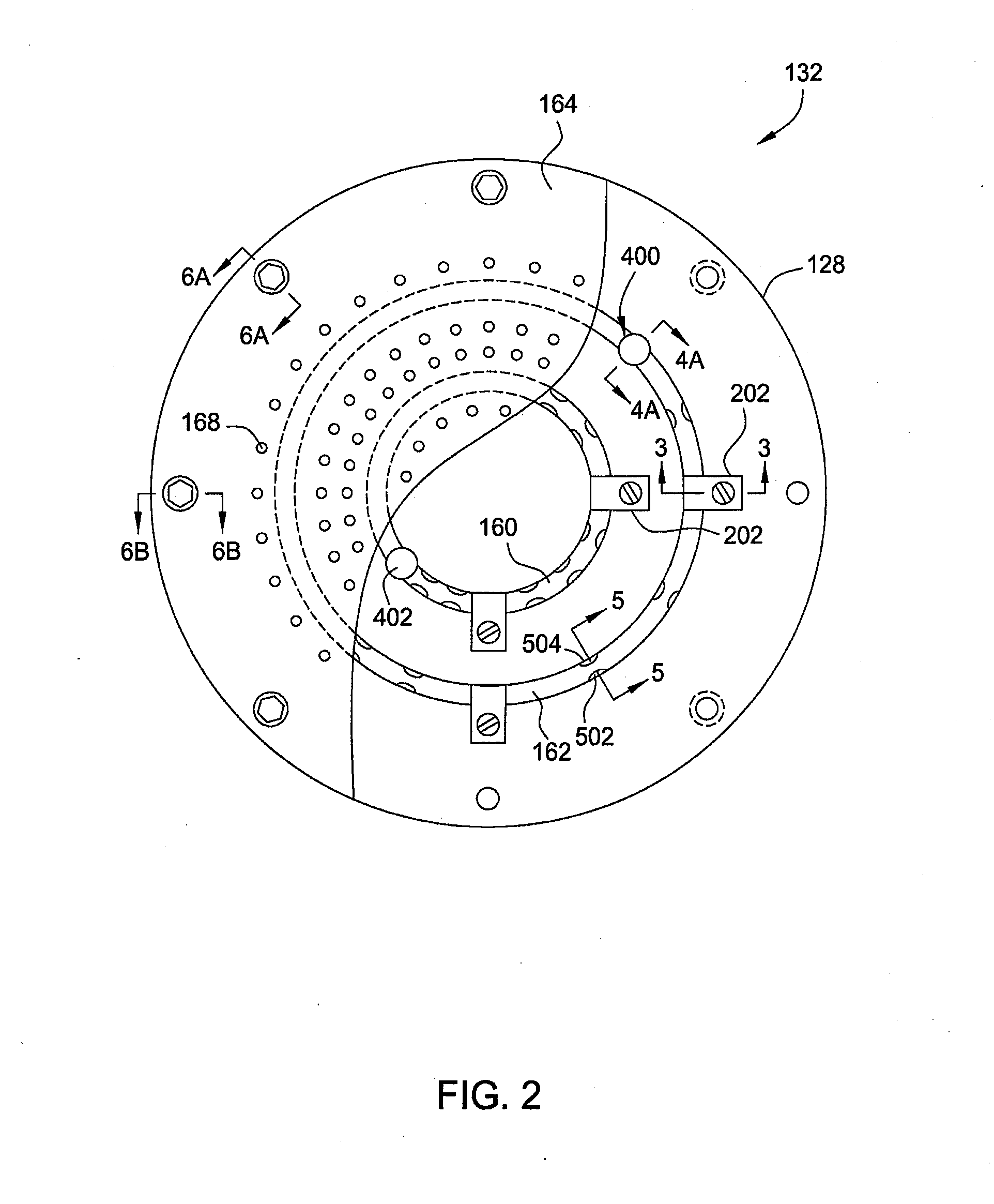
[0025]Embodiments of the present invention generally relate to an apparatus for improving process uniformity across a semiconductor substrate in a plasma processing chamber. Those skilled in the art will understand that other forms of plasma etch chambers may be used to practice the invention, including reactive ion etch (RIE) chambers, electron cyclotron resonance (ECR) chambers, and the like. Furthermore, embodiments of the present invention may be useful in any processing chamber where flow control may improve process uniformity across the surface of a substrate during processing, such as atomic layer deposition (ALD) chambers, chemical vapor deposition (CVD) chambers, plasma enhanced chemical vapor deposition (PECVD) chambers, magnetically enhanced plasma processing chambers, and the like.

[0026]FIG. 1 depicts a schematic, cross-sectional diagram of vacuum processing chamber 102 having a gas diffuser 132 in accordance to an embodiment of the present invention. In the embodiment i...


PUM

PropertyMeasurementUnit
frequencyaaaaaaaaaa
poweraaaaaaaaaa
poweraaaaaaaaaa

Abstract

A method and apparatus for providing flow into a processing chamber are provided. In one embodiment, a vacuum processing chamber is provided that includes a chamber body having an interior volume, a substrate support disposed in the interior volume and a gas distribution assembly having an asymmetrical distribution of gas injection ports. In another embodiment, a method for vacuum processing a substrate is provided that includes disposing a substrate on a substrate support within in a processing chamber, flowing process gas into laterally into a space defined above a gas distribution plate positioned in the processing chamber over the substrate, and processing the substrate in the presence of the processing gas.

Description

BACKGROUND[0001]1. Field of the Invention[0002]Embodiments of the present invention relate to a semiconductor substrate processing system. More particularly, embodiments of the invention relate to a gas flow diffuser for controlling the flow of gases within a semiconductor substrate processing chamber.[0003]2. Background of the Related Art[0004]Integrated circuits have evolved into complex devices that can include millions of components (e.g., transistors, capacitors, resistors, and the like) on a single chip. The evolution of chip designs continually requires faster circuitry and greater circuit density. The demands for greater circuit density necessitate a reduction in the dimensions of the integrated circuit components. The minimal dimensions of features of such devices are commonly referred to in the art as critical dimensions. The critical dimensions generally include the minimal widths of the features, such as lines, columns, openings, spaces between the lines, and the like.[0...

Claims


Application Information

Patent Timeline
Patent Type & Authority Applications(United States)
IPC IPC(8): H01L21/306C23F1/00F16L41/00
CPCC23C16/45502C23C16/45565H01L21/67069H01J37/32449H01J37/3244Y10T137/85938H01L21/02H01L21/3065
Inventor BRILLHART, PAULHOFFMAN, DANIEL J.CARDUCCI, JAMES D.ZHOU, XIAOPINGMILLER, MATTHEW L.
Owner APPLIED MATERIALS INC
Why Eureka
Try Eureka