

Silicon carbide semiconductor device, and method of manufacturing the same
a technology of silicon carbide and semiconductor devices, which is applied in the direction of semiconductor/solid-state device manufacturing, semiconductor devices, electrical equipment, etc., can solve the problems of gate insulation film destruction and use difficulties
- Summary
- Abstract
- Description
- Claims
- Application Information
AI Technical Summary
Benefits of technology
Problems solved by technology
Method used
Image

Examples
first embodiment
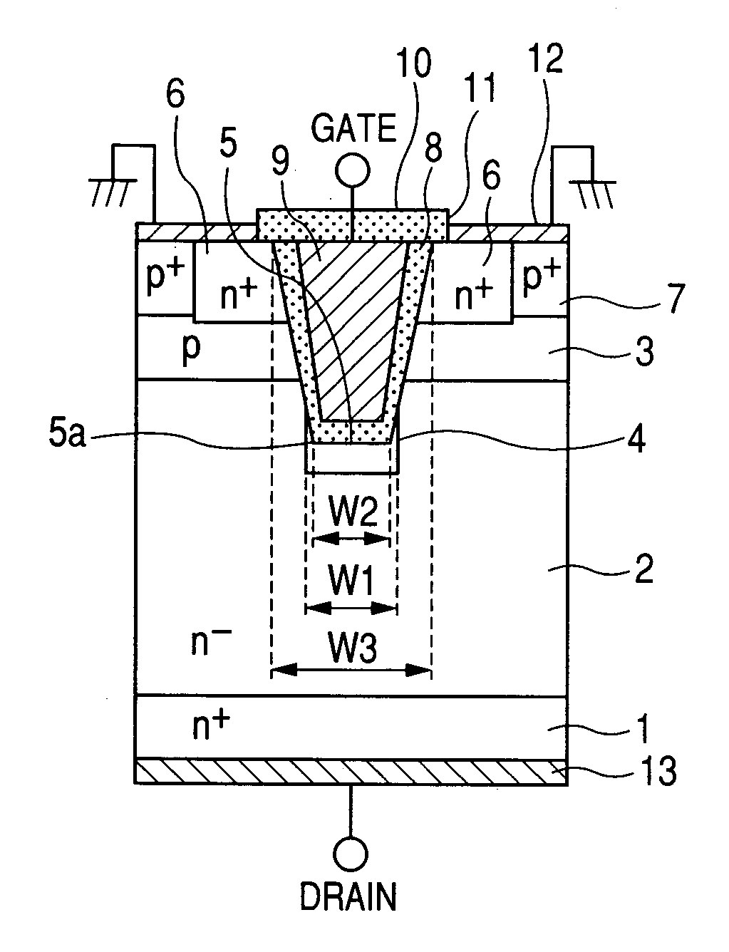
[0135]FIG. 1 is a diagram showing a cross-section of a trench-gate type inverted MOSFET (referred to simply as a MOSFET hereinafter) as a SiC semiconductor device including a vertical power device according to a first embodiment of the invention.
[0136]As shown in FIG. 1, a planar type MOSFET and its circumferential portion are formed on a major surface of an n+-type substrate 1 having a thickness of about 300 μm. The n+-type substrate 1 has an impurity concentration of about 1×1019 cm−3. As n-type impurities of the substrate 1, phosphorus may be used.
[0137]On the major surface of the substrate 1, there is formed an n-type semiconductor layer 2 by epitaxial growth. The n-type semiconductor layer 2 is formed to have an impurity concentration of about 1×1016 cm−3, and a thickness of 10 μm. As n-type impurities of the n-type semiconductor layer 2, phosphorus may be used.
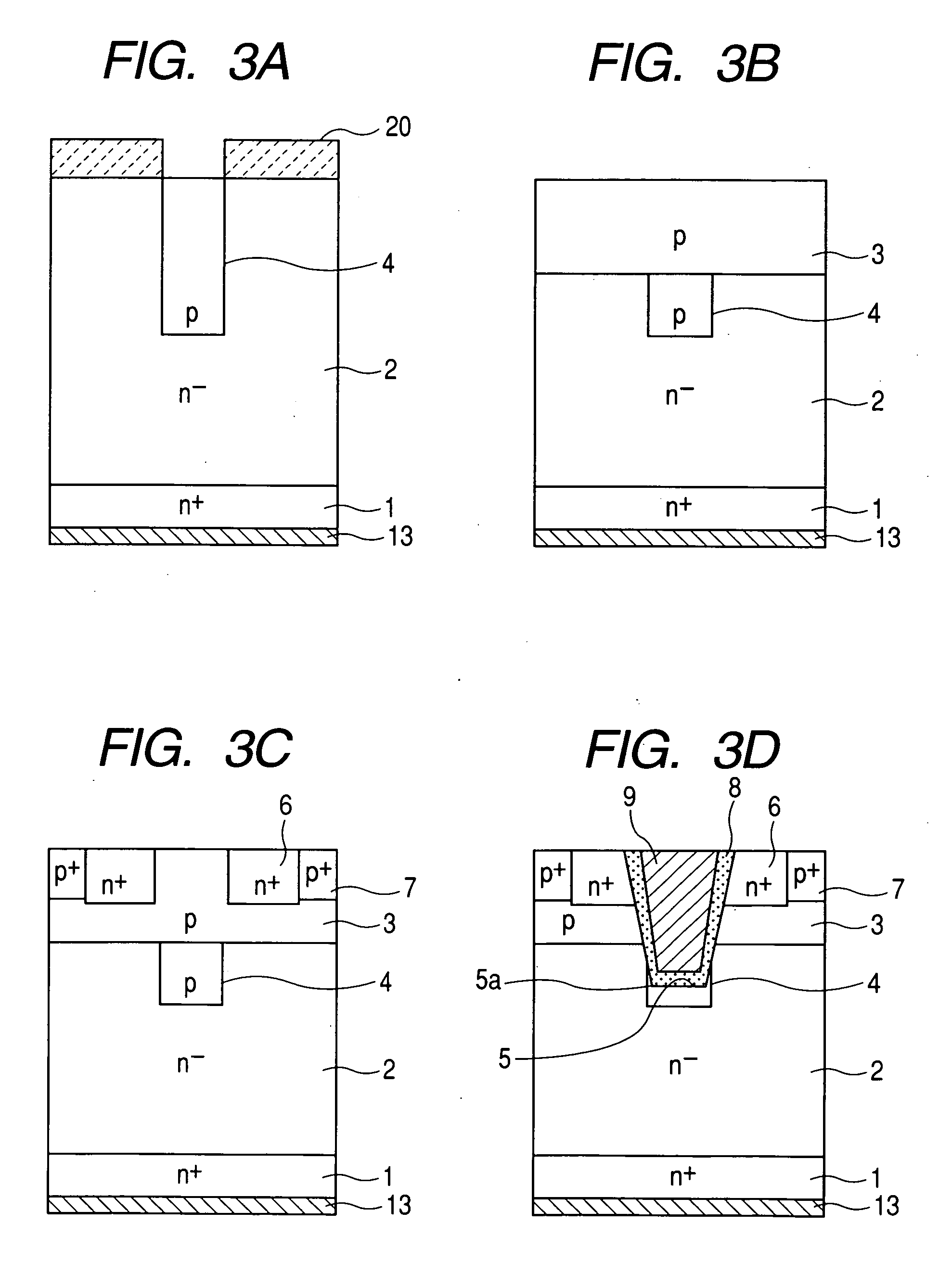
[0138]In the surface portion of the n-type semiconductor layer 2, a plurality of p-type base regions 3 are formed at p...
second embodiment
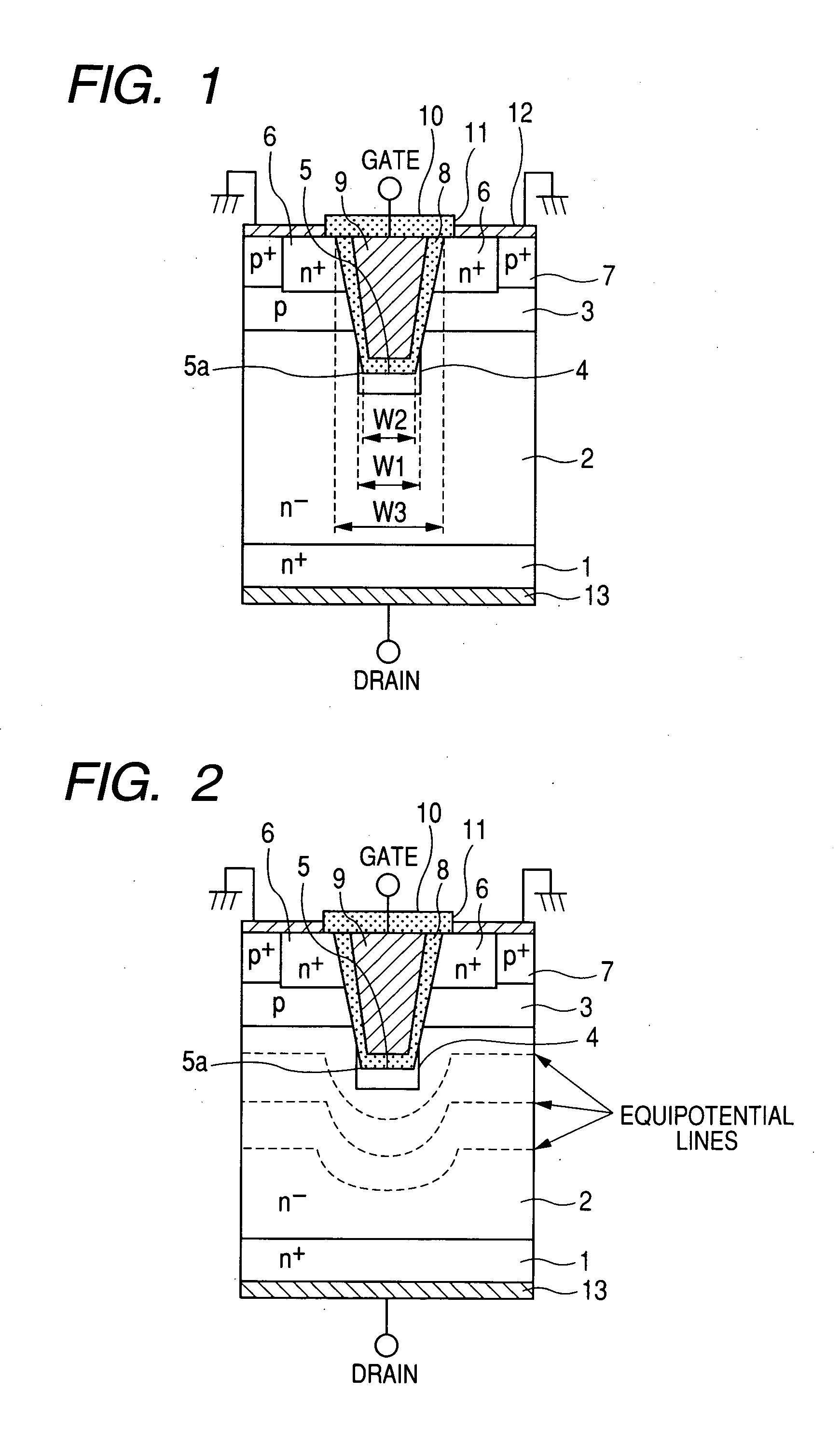
[0160]Next, a second embodiment of the present invention is described. The second embodiment differs from the first embodiment in that the MOSFET of the second embodiment is not an inverted MOSFET but an accumulation-mode MOSFET. The following description on the second embodiment focuses on this difference.
[0161]FIG. 4 is a cross-sectional view of an accumulation-mode MOSFET according to the second embodiment. As shown in FIG. 4, in this embodiment, an n-type channel layer 30 is located so as to be the inner wall of the trench 5. The n-type channel layer 30 is formed so as to connect between the n-type semiconductor layer 2 and the n+-type source regions 6. In this embodiment, the n-type channel layer 30 extends to the bottom surface of the trench 5 to be in contact with the p-type deep layer 4, so that a portion of the inner wall of the trench 5, which is located throughout beneath the n+-type source regions 6 is constituted by the n-type channel layer 30. The p-type deep layer 4 h...
third embodiment
[0173]Next, a third embodiment of the present invention is described. The third embodiment differs from the second embodiment in the depth of the p-type base regions 3. The following description on the third embodiment focuses on this difference.
[0174]FIG. 8 is a cross-sectional view of an accumulation-mode MOSFET according to the third embodiment. FIG. 9 is a diagram showing how a depletion layer extends, and showing equipotential lines in this MOSFET. As shown in FIG. 8, the p-type base regions 3 have the same depth with the p-type deep layer 4.
[0175]The MOSFET of the third embodiment operates in about the same way with the MOSFET of the second embodiment. However, the equipotential lines in this embodiment are parallel to the substrate surface. Accordingly, in this embodiment, a depletion layer extends beneath the p-type base regions 3 and the p-type deep layer 4 in the direction parallel to the substrate surface. This makes it possible to suppress the electric field concentratio...
PUM
 Abstract
Description
Claims
Application Information