Construction of flash memory chips and circuits from ordered nanoparticles

a technology of ordered nanoparticles and flash memory chips, applied in the field of nanoparticles and nanotechnology, fabrication of nanoparticles, fabrication of patterned and ordered nanoparticles and devices, can solve the problems of volatile semiconductor memory devices losing data stored therein, less desirable for embodied high-integrated memory devices, and relatively slow response speed, etc., to achieve uniformly spaced nanoparticles and large periodic arrays

Active Publication Date: 2008-09-25
BOARD OF RGT NEVADA SYST OF HIGHER EDUCATION ON BEHALF OF THE UNIV OF NEVADA RENO
View PDF35 Cites 25 Cited by
  • Summary
  • Abstract
  • Description
  • Claims
  • Application Information

AI Technical Summary

Problems solved by technology

By contrast, NOR flash memory enables random access but, due to a contact pattern formation for each cell transistor, is less desirable for embodying highly integrated memory devices.
However, the volatile semiconductor memory devices lose data stored therein when power is shut off.
Although non-volatile semiconductor memory devices, such as electrically erasable programmable read only memory (EEPROM) devices and / or flash memory devices, have a relatively slow response speed, non-volatile semiconductor memory devices can maintain data stored therein when power is shut off.
Further, leakage current characteristic through the dielectric film is deteriorated.
However, as component dimensions continue to shrink, the surface area of floating gates also shrinks.
This leads directly to a decrease in capacitance of the effective capacitor formed between the floating gate layer and the control gate layer.
The poorly-coupled voltage to floating gate limits the programming and accessing speed characteristics of the memory device.
The present commercial systems and techniques for the manipulation of molecules and atoms into small masses, such as those associated with nanotechnology is still too high an order of complexity today for existing mass production techniques to be applied to nanotechnology.
These techniques allow production of only a low yield of carbon nanotubes, and the population of carbon nanotubes exhibits significant variations in structure and size.
A major challenge facing nanotechnology today is the fabrication of electronic and photonic devices in a commercially viable manner.

Method used


Image

  • Construction of flash memory chips and circuits from ordered nanoparticles
  • Construction of flash memory chips and circuits from ordered nanoparticles
  • Construction of flash memory chips and circuits from ordered nanoparticles

Examples


Embodiment Construction

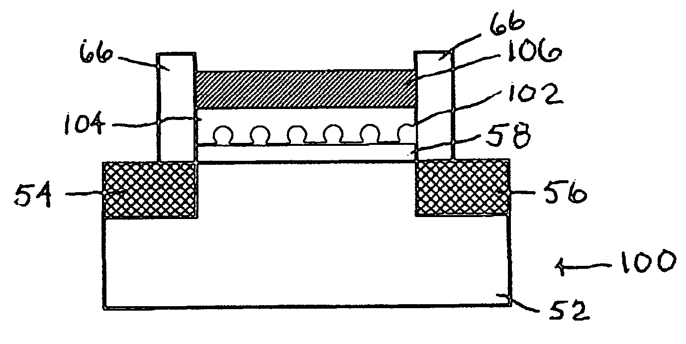
[0041]Flash memory is a very important memory in the semiconductor industry. Flash memory have been broadly applied to replicatively access data but not disappear as power is lost, such as the film of digital camera or the basic input-output system of a mother board, because flash memory has the advantages of electrically erasable and programmable mechanisms. Accordingly, how to advance the performance and reduce the cost of the flash memory becomes an important subject.

[0042]In the conventional method for forming a flash memory cell, the isolation oxide is formed and then a planarization process is performed, such as a chemical mechanism polishing (CMP) process. In the process steps, the CMP process is difficult controlled and the common disadvantages is dishing or erosion on the surface. Hence, there are many solutions to overcome the disadvantages of the CMP process. Moreover, it is more and more important to integrate the processes and to increase the efficiency of the flash mem...


PUM


Abstract

Methods, apparatus and systems form memory structures, such as flash memory structures from nanoparticles by providing a source of nanoparticles as a conductive layer. The particles are moved by application of a field, such as an electrical field, magnetic field and even electromagnetic radiation. The nanoparticles are deposited onto an insulating surface over a transistor in a first distribution of the nanoparticles. A field is applied to the nanoparticles on the surface that applies a force to the particles, rearranging the nanoparticles on the surface by the force from the field to form a second distribution of nanoparticles on the surface. A protective and enclosing insulating layer is deposited on the nanoparticle second distribution. The addition of a top conductive layer completes a basic flash memory structure.

Description

RELATED APPLICATIONS DATA[0001]The present application claims priority from U.S. Provisional Application U.S. Ser. No. 60 / 906,396, which application is incorporate herein by reference in its entirety.BACKGROUND OF THE INVENTION[0002]1. Field of the Invention[0003]The present invention relates to the field of nanoparticles and nanotechnology, fabrication of nanotechnology, fabrication of patterned and ordered nanotechnology and devices, and fabrication of memory devices such as flash memory devices from the ordered nanoparticles. The invention also relates to the field of fabrication of electronic, electrical and photonic devices using nanotechnology.[0004]2. Background of the Art[0005]A flash memory device is a nonvolatile memory device. Depending on a cell array configuration, the flash memory device may be formed as a NAND flash device, which requires no contact pattern to connect each cell transistor, or a NOR flash device, which has contact patterns for each cell transistor. NAN...

Claims


Application Information

Patent Timeline
Patent Type & Authority Applications(United States)
IPC IPC(8): H01L29/788H01L21/28
CPCB82Y10/00H01L21/28273H01L27/115Y10S977/785H01L29/7887Y10S977/936Y10S977/774H01L27/11521H01L29/40114H10B69/00H10B41/30
Inventor T
Owner BOARD OF RGT NEVADA SYST OF HIGHER EDUCATION ON BEHALF OF THE UNIV OF NEVADA RENO
Why Eureka
Try Eureka