Testing method using a scalable parametric measurement macro

a parametric measurement and macro technology, applied in the field of testing methods, can solve the problems of inability to easily use parametric measurements taken during in-line testing to disposition semiconductor products during final testing, and inability to easily identify parametric impact on product yield. the effect of test tim

Inactive Publication Date: 2008-09-25
IBM CORP
View PDF38 Cites 32 Cited by
  • Summary
  • Abstract
  • Description
  • Claims
  • Application Information

AI Technical Summary

Benefits of technology

[0012]Additionally, these in-line to post manufacture parametric measurement correlations can be used to customize future post-manufacture testing. Specifically, these correlations can be stored along with the results of current in-line testing. Prior to final test, both the in-line to post manufacture parametric measurement correlations and the current in-line test results can be accessed and used to determine which chip sites should be used for final test. That is, the current in-line test results and in-line to post manufacture parametric measurement correlations can be used to customize final testing. Specifically, based on theses correlations the accuracy of the various in-line parametric measurements is better understood. Thus, for example, if a given in-line measurement is generally considered to be very accurate in light of the correlations and a current measurement is considered “bad” based on a predetermined criterion, then the chip site where that current measurement was taken can be considered a “known bad site” and can be removed from post-manufacture testing in order to save test-time.

Problems solved by technology

However, parametric deviations are typically not measured post manufacture (i.e., during wafer-level testing, module-level testing, burn-in level testing, etc.), but rather are only measured during in-line testing.
Unfortunately, for a number of reasons, the parametric measurements taken during in-line testing cannot readily be used to disposition semiconductor products during final testing.
Additionally, for a number of reasons, these in-line parametric measurements can also not readily be used to identify parametric impact on product yield.
Thus, unlike prior art Maverick screening methods, neither entire lots, nor entire wafers, which may include good chips, are ever scrapped.

Method used


Image

  • Testing method using a scalable parametric measurement macro
  • Testing method using a scalable parametric measurement macro
  • Testing method using a scalable parametric measurement macro

Examples


Embodiment Construction

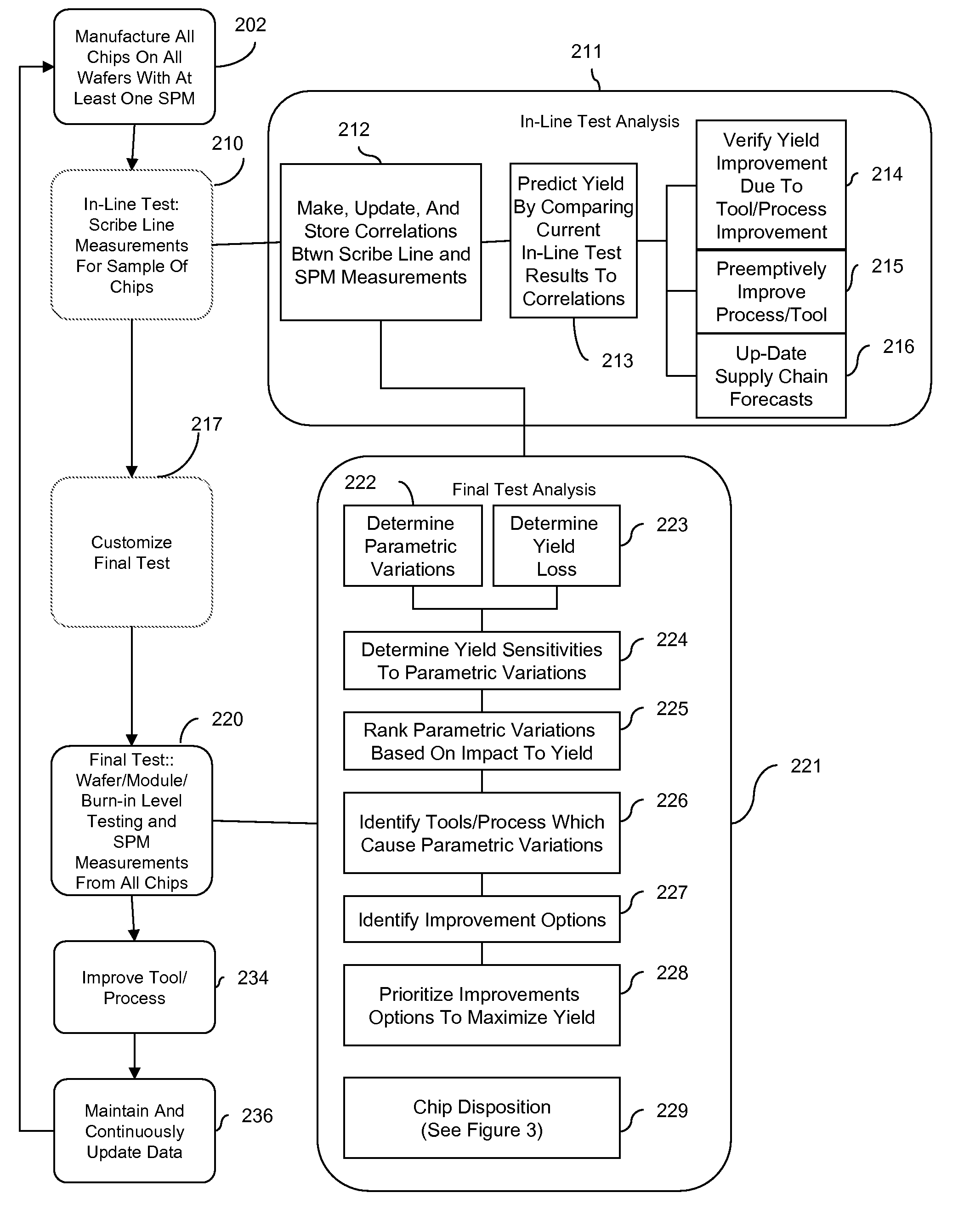
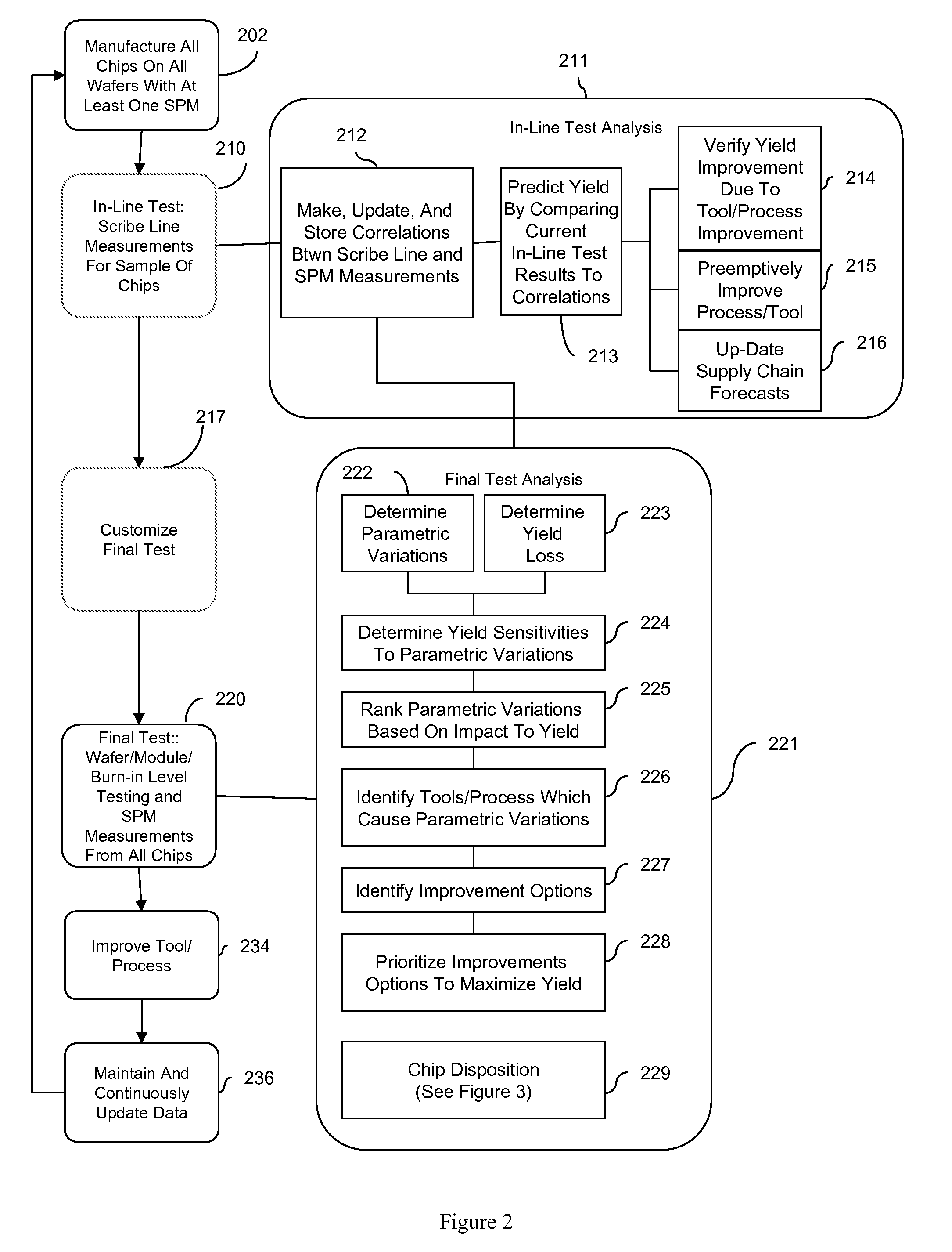
[0020]The embodiments of the invention and the various features and advantageous details thereof are explained more fully with reference to the non-limiting embodiments that are illustrated in the accompanying drawings and detailed in the following description. It should be noted that the features illustrated in the drawings are not necessarily drawn to scale. Descriptions of well-known components and processing techniques are omitted so as to not unnecessarily obscure the embodiments of the invention. The examples used herein are intended merely to facilitate an understanding of ways in which the embodiments of the invention may be practiced and to further enable those of skill in the art to practice the embodiments of the invention. Accordingly, the examples should not be construed as limiting the scope of the embodiments of the invention.

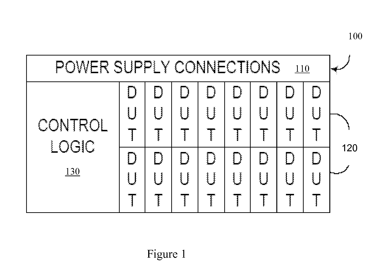
[0021]As mentioned above, semiconductor chips (i.e., dies, semiconductor products, integrated circuit devices, etc.) are generally produced by u...


PUM


Abstract

Disclosed are testing method embodiments in which, during post-manufacture testing, parametric measurements are taken from on-chip parametric measurement elements and used to optimize manufacturing in-line parametric control learning and/or to optimize product screening processes. Specifically, these post-manufacture parametric measurements can be used to disposition chips without shipping out non-conforming products, without discarding conforming products, and without requiring high cost functional tests. They can also be used to identify yield sensitivities to parametric variations from design and to provide feedback for manufacturing line improvements based on the yield sensitivities. Additionally, a historical database regarding the key parameters that are monitored at both the fabrication and post-fabrication levels can be used to predict future yield and, thereby, to preemptively improve the manufacturing line and/or also to update supply chain forecasts.

Description

BACKGROUND[0001]1. Field of the Invention[0002]The embodiments of the invention generally relate to testing methods and, more particularly, to taking parametric measurements during post-manufacture testing of chips in order to optimize manufacturing in-line parametric control learning and / or to optimize product screening processes.[0003]2. Description of the Related Art[0004]Generally, semiconductor chips (i.e., semiconductor products, dies, integrated circuit devices, etc.) are produced by using known processing techniques to form multiple identical products on the same wafer. Deviations in parametric measurements from what is assumed during design, either in different areas across the wafer and / or within different areas across individual chips, impact semiconductor product function in customer applications. However, parametric deviations are typically not measured post manufacture (i.e., during wafer-level testing, module-level testing, burn-in level testing, etc.), but rather are...

Claims


Application Information

Patent Timeline
Patent Type & Authority Applications(United States)
IPC IPC(8): G01R31/26
CPCG01R31/2831G01R31/30G01R31/2894
Inventor BICKFORD, JEANNE P.GOSS, JOHN R.HABIB, NAZMULMCMAHON, ROBERT J.
Owner IBM CORP
Why Eureka
Try Eureka