Method of fabricating GaN LED

a technology of gallium nitride and light-emitting diodes, which is applied in the direction of basic electric elements, electrical apparatus, semiconductor devices, etc., can solve the problems of poor crystal interface quality, deformation of device quality, and difficulty in mass production, so as to reduce the density of gan defects, improve the light-emitting efficiency of the device, and improve the effect of crystal interface quality

Inactive Publication Date: 2008-09-25
NAT SUN YAT SEN UNIV +1
View PDF5 Cites 12 Cited by
  • Summary
  • Abstract
  • Description
  • Claims
  • Application Information

AI Technical Summary

Benefits of technology

[0006]The main purpose of the present invention is to use a ZnO buffer layer to successfully grow a GaN nucleus-site layer as a single crystal thin film on a LiAlO2 substrate for reducing GaN defect density and for further obtaining lattice match to have a good crystal interface quality and an enhanced light emitting efficiency of a device thus made

Problems solved by technology

Thus, crystal interface quality become bad and quality of a device thus made is degraded.
And such a situation makes mass production difficult.
Hence, the prior arts do not fulfill all users' requests on actual use.

Method used


Image

  • Method of fabricating GaN LED
  • Method of fabricating GaN LED
  • Method of fabricating GaN LED

Examples


Embodiment Construction

[0018]The following description of the preferred embodiment is provided to understand the features and the structures of the present invention.

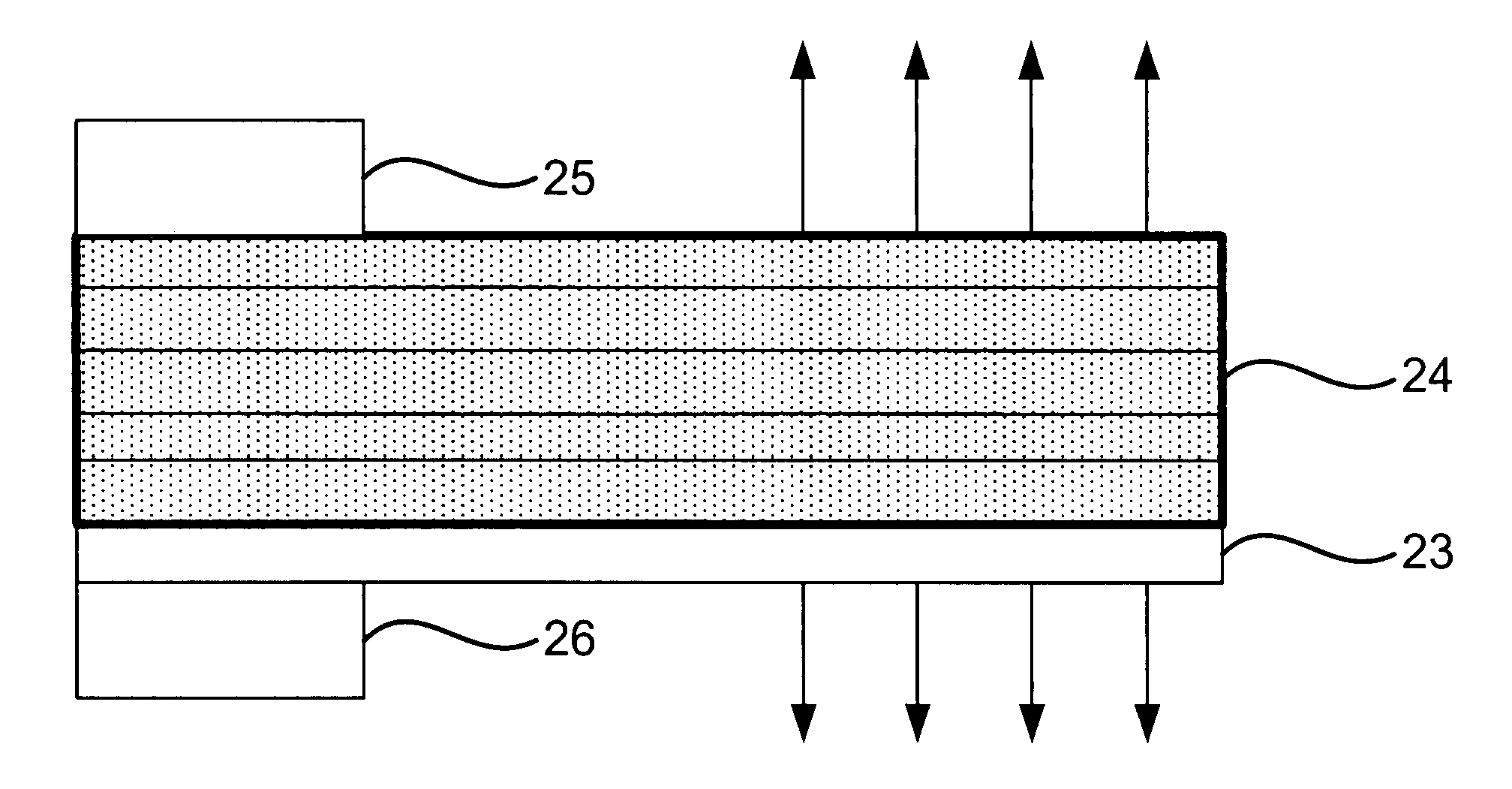
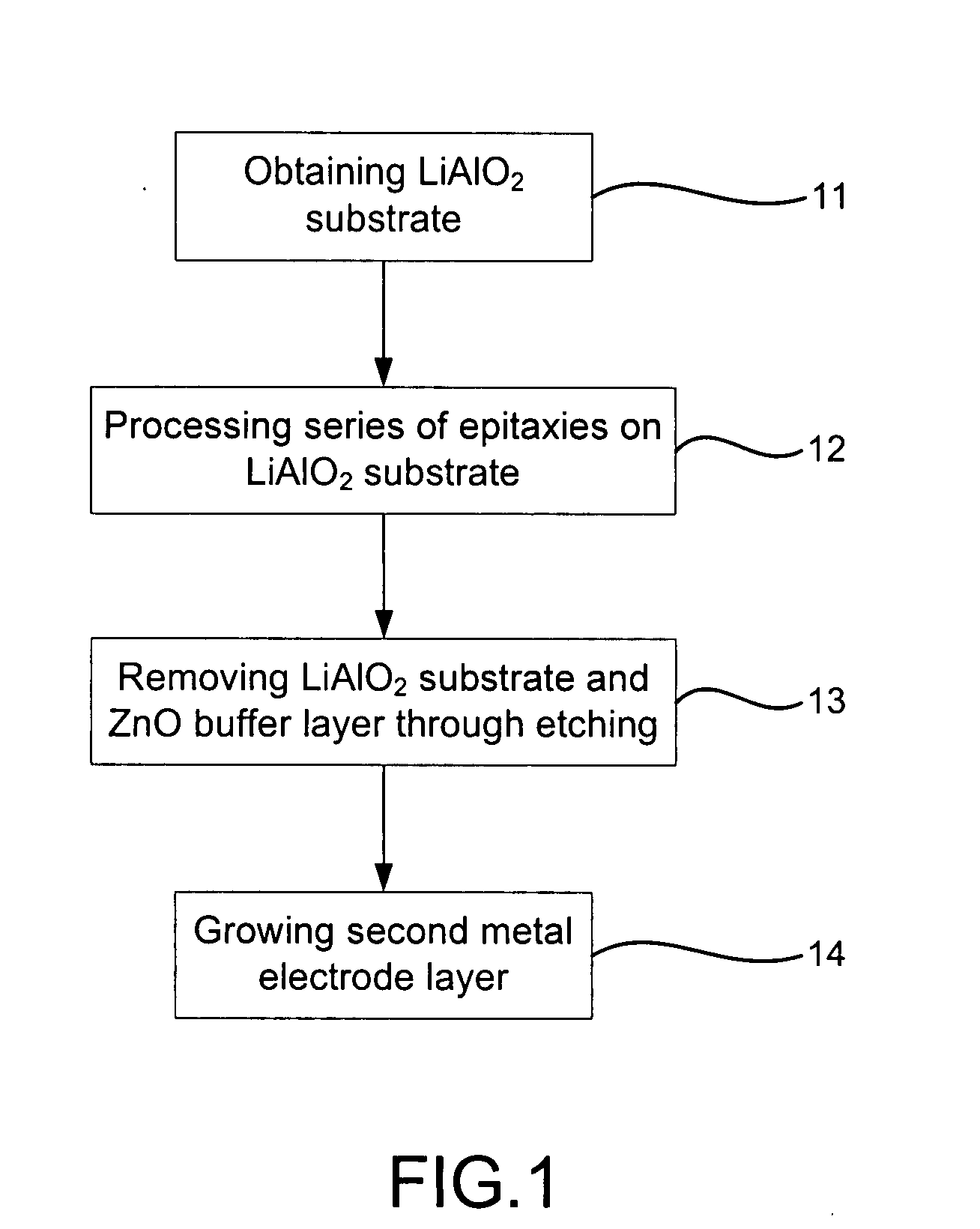
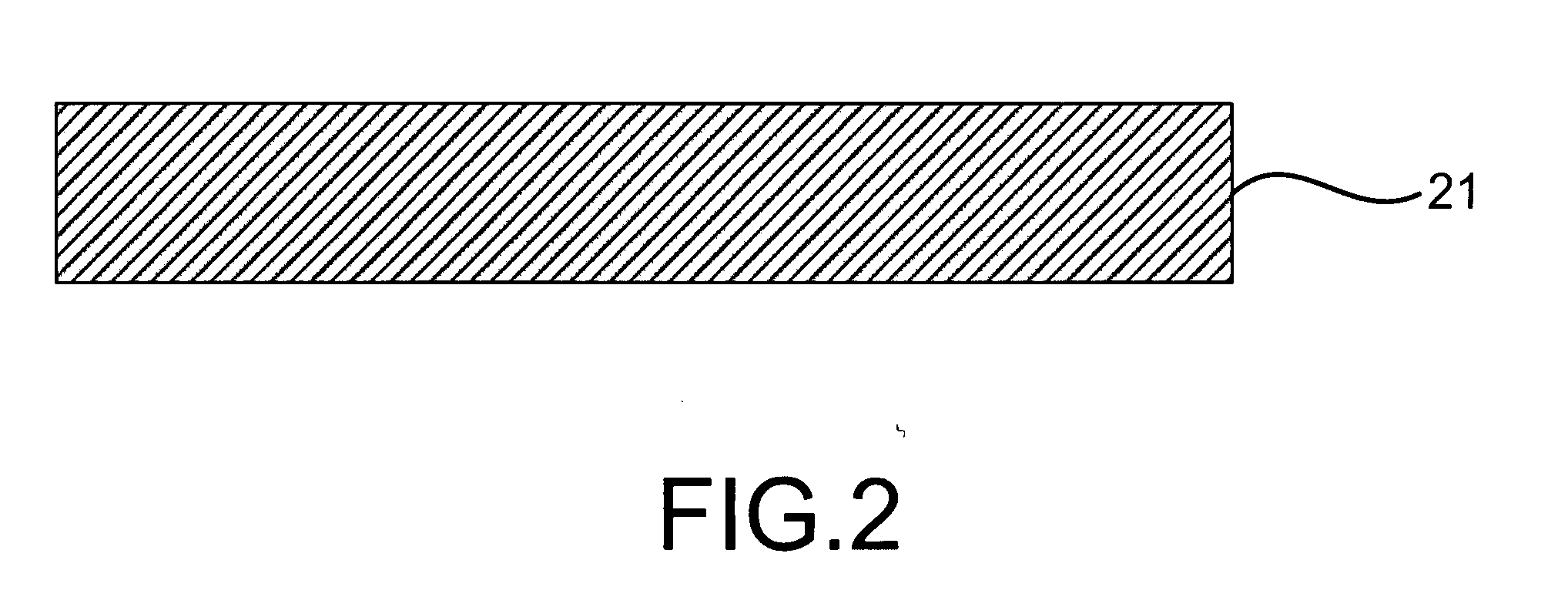
[0019]Please refer to FIG. 1 to FIG. 5, which are a flow view showing a preferred embodiment according to the present invention; a view showing a LiAlO2 substrate; a view showing a structure after a series of epitaxy; a view showing a structure after etching the LiAlO2 substrate and a ZnO buffer layer; and a view showing a LED. As shown in the figures, the present invention is a method of fabricating a gallium nitride (GaN) light emitting diode (LED), comprising the following steps:

[0020](a) Obtaining a LiAlO2 substrate 11: As shown in FIG. 2, a substrate of lithium aluminum oxide (LiAlO2) 21 is obtained. The substrate can further be a substrate of lithium gallium oxide (LiGaO2), lithium silicon oxide (Li2SiO3), lithium germanium oxide (LiGeO3), sodium aluminum oxide (NaAlO2), sodium germanium oxide (Na2GeO3), sodium silicon oxide (Na2SiO3), ...


PUM


Abstract

A light emitting diode (LED) is made. The LED had a LiAlO2 substrate and a GaN layer. Between them, there is a zinc oxide (ZnO) layer. Because GaN and ZnO have a similar. Wurtzite structure, GaN can easily grow on ZnO. By using the ZnO layer, the GaN layer is successfully grown as a single crystal thin film on the LiAlO2 substrate. Thus, GaN defect density is reduced and lattice match is obtained to have a good crystal interface quality and an enhanced light emitting efficiency of a device thus made.

Description

FIELD OF THE INVENTION[0001]The present invention relates to fabricating a gallium nitride (GaN) light emitting diode (LED); more particularly, relates to using a zinc oxide (ZnO) buffer layer to successfully grow a GaN nucleus-site layer as a single crystal thin film on a lithium aluminum oxide (LiAlO2) substrate for reducing GaN defect density and for further obtaining lattice match to have a good crystal interface quality and an enhanced light emitting efficiency of a device thus made.DESCRIPTION OF THE RELATED ARTS[0002]A traditional LED usually uses a sapphire substrate to grow GaN. As shown in FIG. 7 and FIG. 8, a sapphire substrate 31 is obtained to grow a GaN multiple quantum well (MQW) 32 and then a p-side electrode layer 33. And then an n-side electrode layer 34 is grown at another side on the GaN MQW 32. Thus, a LED is made.[0003]However, its electroluminescence spectrum is controlled by the quantum wells near the p-side electrode layer 33, emitting a non-uniformed white ...

Claims


Application Information

Patent Timeline
Patent Type & Authority Applications(United States)
IPC IPC(8): H01L21/02
CPCH01L33/0079H01L33/007H01L33/0093
Inventor CHOU, MITCH M. C.WU, JIH-JENHSU, WEN-CHING
Owner NAT SUN YAT SEN UNIV
Why Eureka
Try Eureka