Semiconductor integrated circuit device

a technology of integrated circuit devices and semiconductors, applied in the direction of near-field systems using receivers, mechanical actuation of burglar alarms, instruments, etc., can solve the problems of power source efficiency dropping just, operation as if noise back-scattered may occur, etc., to achieve stable communication without lowering communication efficiency. , the effect of limiting the communication distance in the id tag

Active Publication Date: 2008-10-02
RENESAS ELECTRONICS CORP
View PDF6 Cites 46 Cited by
  • Summary
  • Abstract
  • Description
  • Claims
  • Application Information

AI Technical Summary

Benefits of technology

[0009]Usually, setting for reducing the communication distance is updated using information previously set in a memory or the like from a host in a power-up sequence of the ID tag. However, power source efficiency lowers just after the update, and at this time, if input power is not large sufficiently, the ID tag is powered-off.
[0012]An object of the present invention is to provide a technique capable of limiting a communication distance in the ID tag while realizing stable communication without lowering communication efficiency.
[0027](1) Since communication distance limitation is performed while monitoring a clamp current, the communication distance limitation can be performed at stable operation without lowering communication efficiency.
[0028](2) And, since input of a command is limited when the communication distance limitation is set, it is possible to prevent repetition of ON / OFF of a semiconductor integrated circuit device and noise scattering can be prevented.
[0029](3) According to the above (1) and (2), an RFID system with high reliability can be realized.

Problems solved by technology

However, in the abovementioned techniques of communication response distance reduction utilizing the RFID, following problems are found by the inventors.
However, power source efficiency lowers just after the update, and at this time, if input power is not large sufficiently, the ID tag is powered-off.
Generally, since impedance of a semiconductor device varies depending on existence / nonexistence of bias, magnitude of a reflection wave from the ID tag is fluctuated because of repetition of ON / OFF, and therefore, there is a concern that operation as if noise is back-scattered may occur.

Method used


Image

  • Semiconductor integrated circuit device
  • Semiconductor integrated circuit device
  • Semiconductor integrated circuit device

Examples


first embodiment

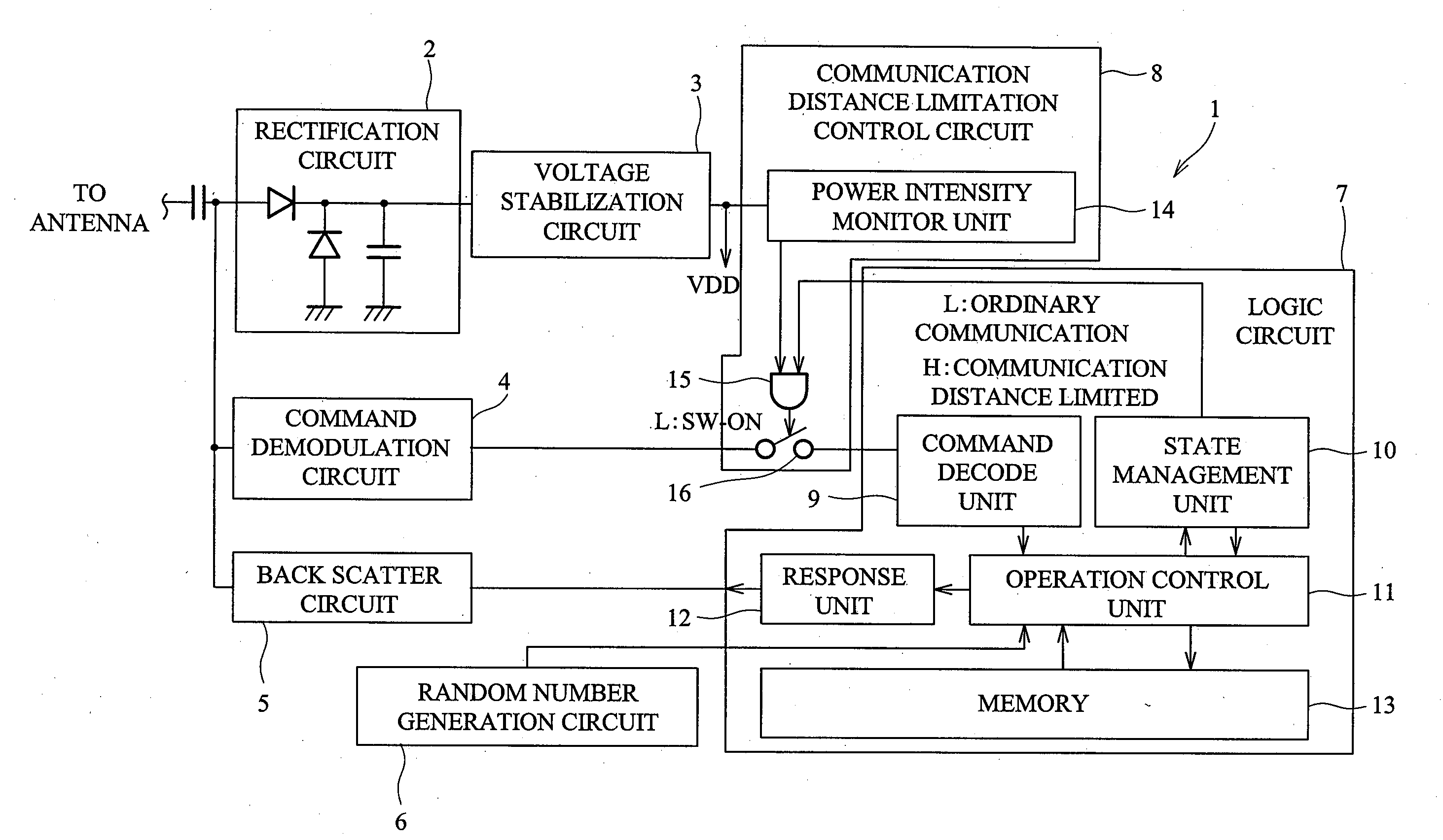
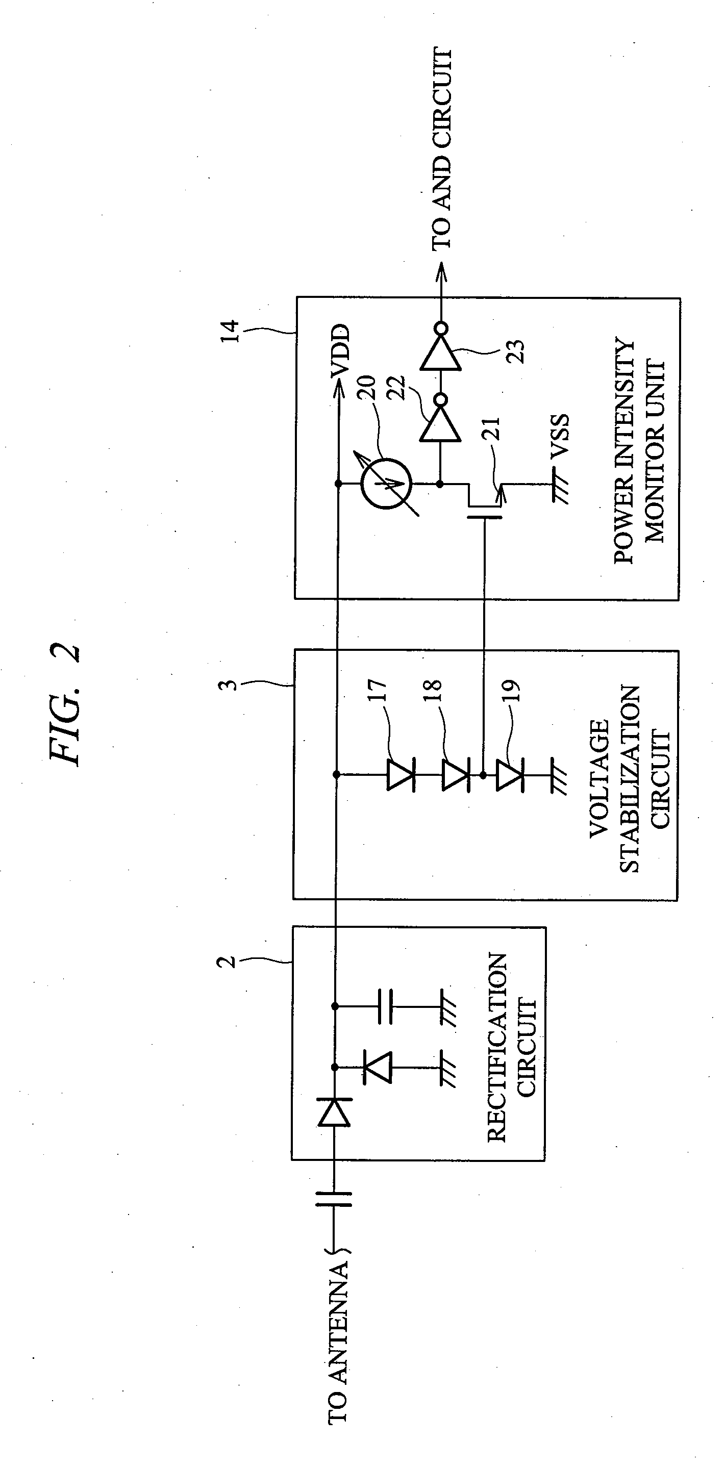
[0036]FIG. 1 is a block diagram of a semiconductor integrated circuit device according to a first embodiment of the present invention, FIG. 2 is an explanatory diagram showing a configuration example of a voltage stabilization circuit and a power intensity monitor unit provided in the semiconductor integrated circuit device shown in FIG. 1, and FIG. 3 is a flowchart showing one example of operation of a communication distance limitation control circuit provided in the semiconductor integrated circuit device shown in FIG. 1.

[0037]In the first embodiment, a semiconductor integrated circuit device 1 is used for, for example, an ID tag of an RFID system which is one of automatic recognition techniques. As shown in FIG. 1, the semiconductor integrated circuit device 1 comprises a rectification circuit 2, a voltage stabilization circuit 3, a command demodulation circuit 4, a back scatter circuit 5, a random number generation circuit 6, a logic circuit 7 and a communication distance limita...

second embodiment

[0073]FIG. 4 is an explanatory diagram showing a configuration example of a voltage stabilization circuit and a power intensity monitor unit provided in a semiconductor integrated circuit device according to a second embodiment of the present invention.

[0074]In the second embodiment, a semiconductor integrated circuit 1 (FIG. 1) comprises a rectification circuit 2, a voltage stabilization circuit 3, a command demodulation circuit 4, a back scatter circuit 5, a random number generation circuit 6, a logic circuit 7 and a communication distance limitation control circuit 8 in the same way as that of the first embodiment. The second embodiment is different from the first embodiment in configurations of the voltage stabilization circuit 3 and the power intensity monitor unit 14.

[0075]FIG. 4 is a block diagram showing a configuration example of the voltage stabilization circuit 3 and the power intensity monitor unit 14.

[0076]The voltage stabilization circuit 3 comprises resistors 24 to 27...


PUM


Abstract

In an IC tag, when a semiconductor integrated circuit device is activated, an operation control unit sets existence / nonexistence of a communication distance limitation for reducing a communication distance to a state management unit. If the communication distance limitation is not set, a switch unit is turned ON and a demodulated command is inputted from a command demodulation circuit to a command decode unit. If the communication distance limitation is set, a power intensity monitor unit judges whether the power of a rectification circuit is a predetermined arbitrary field intensity or more. If the power is smaller than the predetermined arbitrary field intensity, the switch unit is turned OFF and various commands demodulated by the command demodulation circuit are not inputted to the command decode unit. As a result, the semiconductor integrated circuit device does not operate.

Description

CROSS-REFERENCE TO RELATED APPLICATION[0001]The present application claims priority from Japanese Patent Application No. JP 2007-091614 filed on Mar. 30, 2007, the content of which is hereby incorporated by reference into this application.TECHNICAL FIELD OF THE INVENTION[0002]The present invention relates to an RFID (Radio Frequency IDentification) system, and in particular to a technique effective for improvement of security in an ID tag.BACKGROUND OF THE INVENTION[0003]As an automatic recognition technique enabling data transmission through radio communication, RFID is spreading. For example, the RFID comprises an ID tag capable of storing information, a reader / writer performing reading and writing of information in the ID tag and a host performing management of the information read by the reader / writer and the like.[0004]Unique ID information is allocated to each ID tag, and therefore, in commodity distribution and the like, by attaching the ID tag to a commercial product and dis...

Claims


Application Information

Patent Timeline
Patent Type & Authority Applications(United States)
IPC IPC(8): H04B7/00
CPCH04B5/0031H04B5/0037H04B5/02
Inventor ENDO, TAKEFUMITSUKAMOTO, TAKAYUKI
Owner RENESAS ELECTRONICS CORP
Why Eureka
Try Eureka