Catalyst-assisted atomic layer deposition of silicon-containing films with integrated in-situ reactive treatment

a technology of catalyst-based ald and silicon-containing films, which is applied in the direction of resistive material coating, superimposed coating process, thermoelectric devices, etc., can solve the problems of high temperature, low deposition temperature, and many drawbacks of catalyst-based ald of siosub>2 /sub>film in the prior art, so as to reduce or eliminate the need for undetectable high-temperature post-deposition processing

Active Publication Date: 2008-10-02
TOKYO ELECTRON LTD
View PDF6 Cites 47 Cited by
  • Summary
  • Abstract
  • Description
  • Claims
  • Application Information

AI Technical Summary

Benefits of technology

[0011]Embodiments of the invention address the aforenoted need by providing an improved method of low temperature catalyst-assisted deposition of silico

Problems solved by technology

Furthermore, low deposition temperatures are often required, for example due to restricted thermal budget and interlayer diffusion that may destroy the properties of nanoscale devices.
However, these ALD processes are often at temperatures too high to prevent unwanted oxidation of a substrate.
However, catalyst-based ALD of SiO2 film in the prior art suffers from several drawbacks.
For example, chlorine (Cl) and carbon (C) impurities are frequently incorporated into the SiO2 film during deposition, where the carbo

Method used


Image

  • Catalyst-assisted atomic layer deposition of silicon-containing films with integrated in-situ reactive treatment
  • Catalyst-assisted atomic layer deposition of silicon-containing films with integrated in-situ reactive treatment
  • Catalyst-assisted atomic layer deposition of silicon-containing films with integrated in-situ reactive treatment

Examples


Embodiment Construction

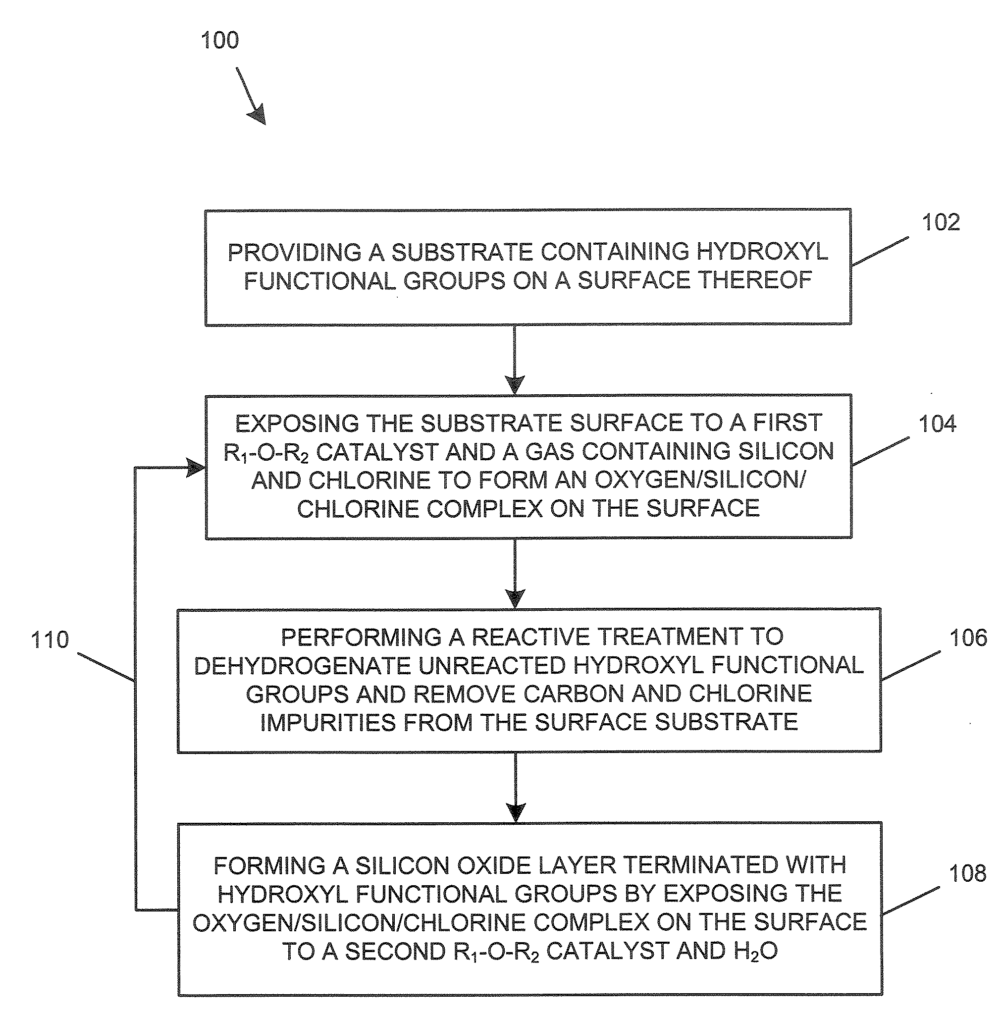
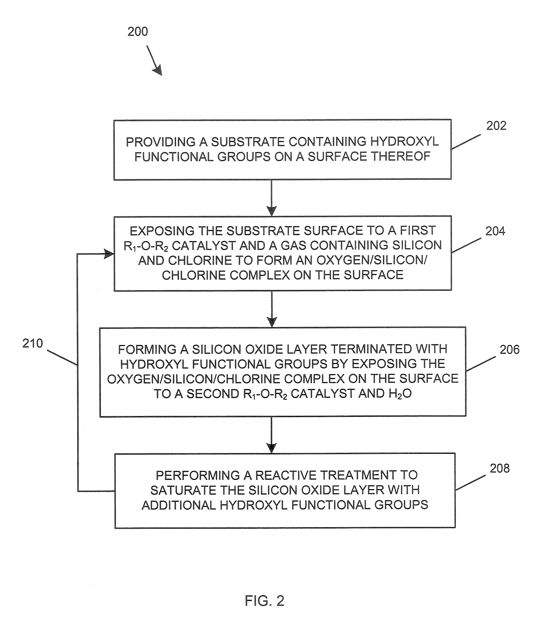
[0019]Embodiments of the invention provide a method of depositing a silicon-containing film on a functionalized substrate at room temperature or near room temperature using catalyst-based ALD integrated with one or more in-situ reactive treatment(s). Due to the reduced impurity levels in the as-deposited silicon-containing films, high-temperature post-deposition processing may be reduced or eliminated, thereby maximizing the benefits gained by the low temperature catalyst-assisted ALD processing provided by embodiments of the invention.

[0020]Using catalyst-assisted ALD of a SiO2 film as an example for a silicon-containing film, catalyzed self-terminating surface reactions applied in a binary reaction sequence have focused on dividing a SiCl4+2H2O→SiO2+4HCl reaction into two half-reactions:

Si—OH*+SiCl4+Catalyst→SiO—Si(—Cl*)3+HCl+Catalyst  (A)

Si—Cl*+H2O+Catalyst→Si—OH*+HCl+Catalyst  (B)

[0021]where the asterisks designate the surface species and the half-reactions are performed in an A...


PUM

PropertyMeasurementUnit
Temperatureaaaaaaaaaa

Abstract

A method is provided for low temperature catalyst-assisted atomic layer deposition of silicon-containing films such as SiO2 and SiN. The method includes exposing a substrate surface containing X—H functional groups to a first R1—X—R2 catalyst and a gas containing silicon and chlorine to form an X/silicon/chlorine complex on the surface, and forming a silicon-X layer terminated with the X—H functional groups by exposing the X/silicon/chlorine complex on the substrate surface to a second R1—X—R2 catalyst and a X—H functional group precursor. The method further includes one or more integrated in-situ reactive treatments that reduce or eliminate the need for undesired high-temperature post-deposition processing. One reactive treatment includes hydrogenating unreacted X—H functional groups and removing carbon and chlorine impurities from the substrate surface. Another reactive treatment saturates the silicon-X layer with additional X—H functional groups.

Description

FIELD OF THE INVENTION[0001]The present invention relates to thin film deposition, and more particularly to low temperature catalyst-assisted deposition of silicon-containing films such as silicon nitride and silicon oxide.BACKGROUND OF THE INVENTION[0002]The reduction of thin films to nanometer dimensions for new technologies requires excellent control of film thickness, morphology, crystallinity, and conformality. Many of these requirements can be achieved by growth controlled at single atomic layers by means of binary reaction sequence chemistry. Furthermore, low deposition temperatures are often required, for example due to restricted thermal budget and interlayer diffusion that may destroy the properties of nanoscale devices. Atomic layer deposition (ALD) may be preferred or required for some advanced manufacturing processes due to its superior conformal deposition and film thickness control, and current ALD processes are often performed at lower temperatures than chemical vapo...

Claims


Application Information

Patent Timeline
IPC IPC(8): B05D5/12
CPCC23C16/345C23C16/402C23C16/45534C23C16/45536
Inventor JOE, RAYMONDGANDHI, MEENAKSHISUNDARAM
Owner TOKYO ELECTRON LTD
Why Eureka
Try Eureka