Method Of Manufacturing Semiconductor

a manufacturing method and semiconductor technology, applied in the direction of semiconductor devices, electrical equipment, transistors, etc., can solve the problems of reducing the useful life of the ion source, ion implantation alone is not sufficient for the formation of an effective semiconductor junction, and the material needed to produce such ions is extremely toxi

Inactive Publication Date: 2008-10-02
SEMEQUIP +1
View PDF11 Cites 23 Cited by
  • Summary
  • Abstract
  • Description
  • Claims
  • Application Information

AI Technical Summary

Benefits of technology

[0012]Briefly, the present invention relates to a method of producing ultra shallow junctions for PMOS transistors without the need for pre-amorphization implants by utilizing B18Hx+ ion implantation to both dope and self- or auto-amorphize a silicon substrate in the region of the source and drain extension. A key element of the present invention is that the pre-amorphizing step may be eliminated, resulting in substantial cost savings in processing a wafer. An appropriate anneal is used to activate the dopant and repair the implant damage. The depth of implantation is controlled by the implant parameters, such as energy, dose and tilt angle. Tilted implants (i.e. “halo” or “pocket” implants) may be used in conjunction with B18Hx+ source / drain extension implants to place the dopant atoms in the appropriate location to elevate the short channel effect. An appropriate process sequence is utilized that compliments the use of B18Hx+ ion implantation. The wafer may be tilted during the source / drain extension B18Hx+ implantation to tailor its profile to enhance transistor performance.

Problems solved by technology

Unfortunately, the feed material needed to produce such ions is extremely toxic and drastically reduces the useful life of the ion source.
In general, ion implantation alone is not sufficient for the formation of an effective semiconductor junction.

Method used


Image

  • Method Of Manufacturing Semiconductor
  • Method Of Manufacturing Semiconductor
  • Method Of Manufacturing Semiconductor

Examples


Embodiment Construction

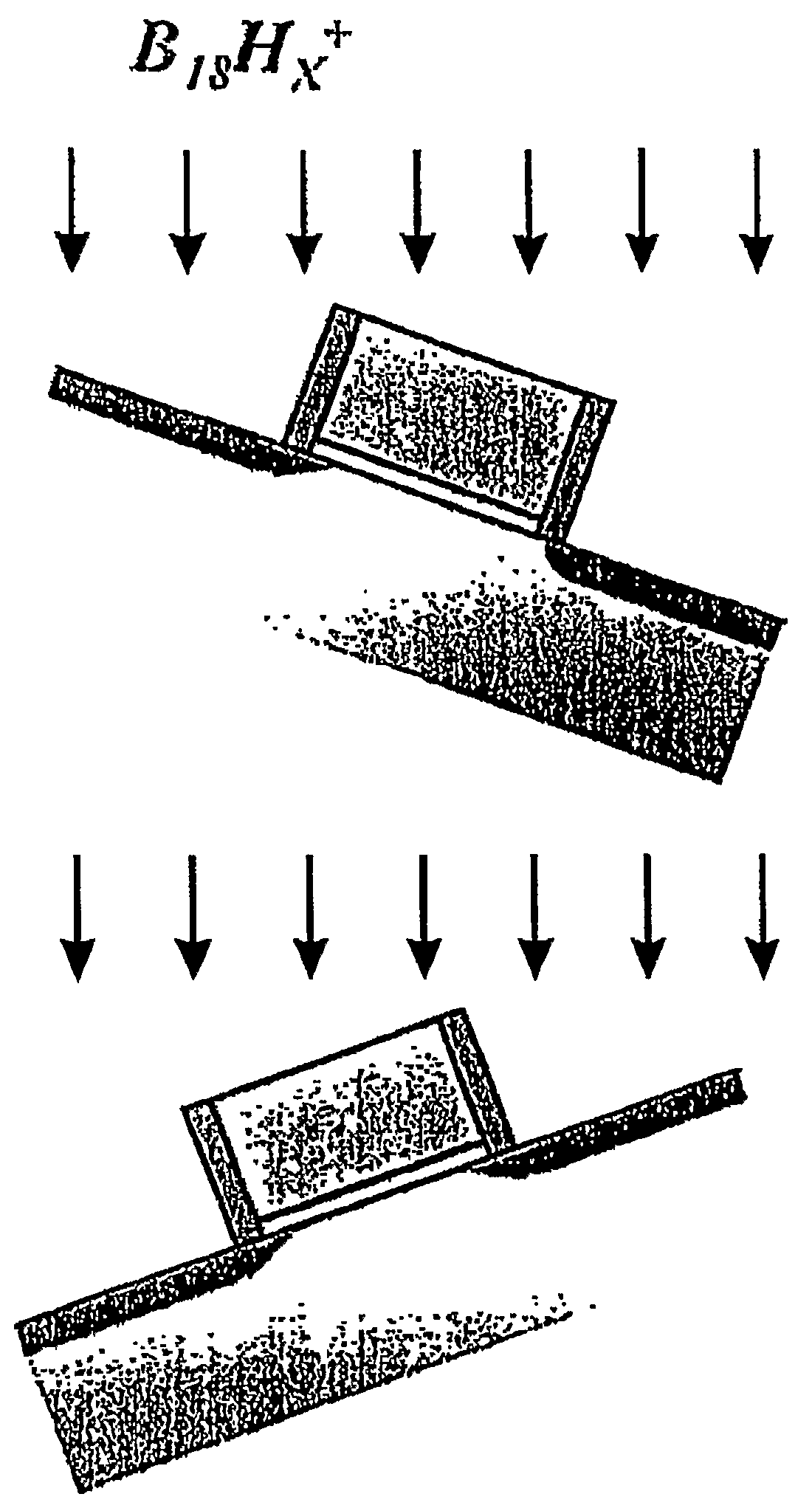
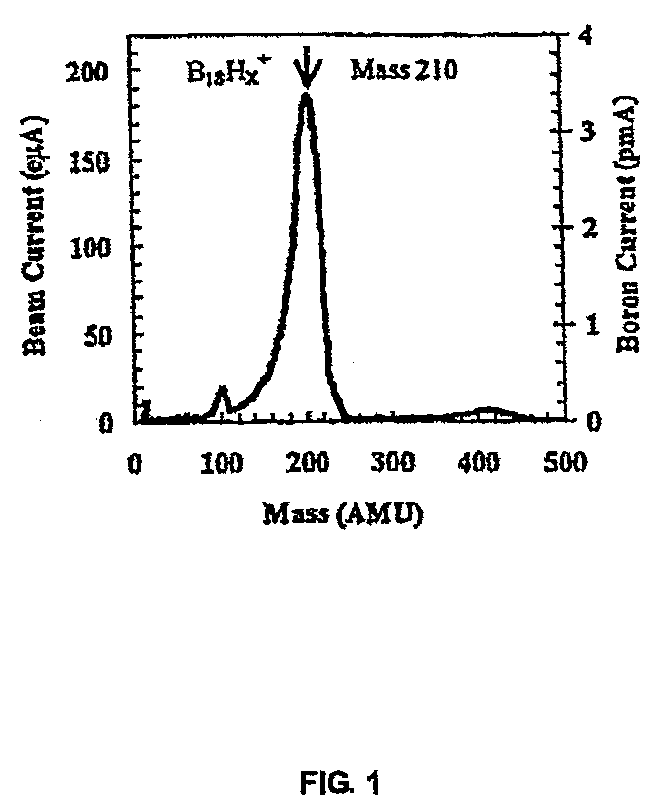
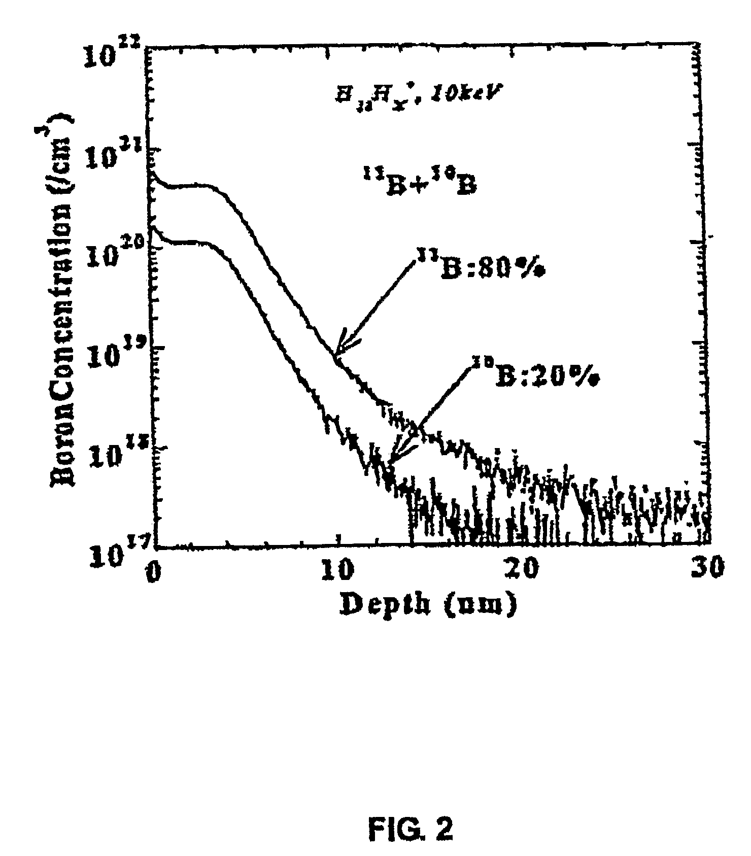
[0026]The present invention relates to a method of producing ultra shallow junctions for PMOS transistors without the need for pre-amorphization implants by utilizing B18Hx+ ion implantation to both dope and self- or auto-amorphize a silicon substrate in the region of the source and drain extension. A key element of the present invention is that the pre-amorphizing step may be eliminated, for example, as illustrated in FIG. 6, resulting in substantial cost savings in processing a wafer. An appropriate anneal is used to activate the dopant and repair the implant damage. The depth of implantation is controlled by the implant parameters, such as energy, dose and tilt angle. Tilted implants (i.e. “halo” or “pocket” implants), for example, as illustrated in FIG. 7, may be used in conjunction with B18Hx+ source / drain extension implants to place the dopant atoms in the appropriate location to elevate the short channel effect. Furthermore an appropriate process sequence is utilized that com...


PUM


Abstract

A method of producing ultra shallow junctions ( 104 ) for PMOS transistors, which eliminates the need for pre-amorphization implants, is disclosed. The method utilizes dopant species, such as cluster ions, e.g., octadecaborane, B18H22. In accordance with the present invention, the pre-amorphizing step may be eliminated, greatly reducing cost per processed wafer. An appropriate process sequence has been suggested to take advantage of cluster ion implantation for PMOS manufacturing. In addition, the novel use of tilted implants for the source / drain extension and for pocket implants has been described.

Description

CROSS REFERENCE TO RELATED APPLICATIONS[0001]This application claims the benefit and priority to U.S. Provisional Patent Application No. 60 / 621,112, filed on Oct. 22, 2004.1. FIELD OF THE INVENTION[0002]The present invention relates to integrated circuit manufacturing with enhanced throughput utilizing ultra-low energy boron implants with improved junction characteristics.2. DESCRIPTION OF THE PRIOR ART[0003]CMOS is the dominant integrated circuit technology in current use and its name denotes the formation of both N-channel and P-channel MOS transistors (Complementary MOS: both N and P) on the same chip. The success of CMOS is that circuit designers can make use of the complementary nature of the opposite transistors to create a better circuit, specifically one that draws less active power than alternative technologies. It is known that the N and P terminology is based on Negative and Positive (N-type semiconductor has negative majority carriers, and vice versa), and the N-channel ...

Claims


Application Information

Patent Timeline
Patent Type & Authority Applications(United States)
IPC IPC(8): H01L21/265
CPCH01L21/26513H01L21/26586H01L21/324H01L21/823814H01L29/1045H01L29/1083H01L29/4933H01L29/665H01L29/6659
Inventor JACOBSON, DALE C.KAWASAKI, YOJI
Owner SEMEQUIP
Why Eureka
Try Eureka