Structure for monitoring semiconductor polysilicon gate profile

a polysilicon gate and gate profile technology, applied in the field of polysilicon lines, can solve the problems of affecting the quality of the gate profile, the shape of the rectangular profile may drift, and the destructive technique of visual detection, so as to facilitate the generation of profile drift statistics, facilitate the regular testing of profile drift, and save significant costs

Inactive Publication Date: 2006-02-02
IBM CORP
View PDF53 Cites 5 Cited by
  • Summary
  • Abstract
  • Description
  • Claims
  • Application Information

AI Technical Summary

Benefits of technology

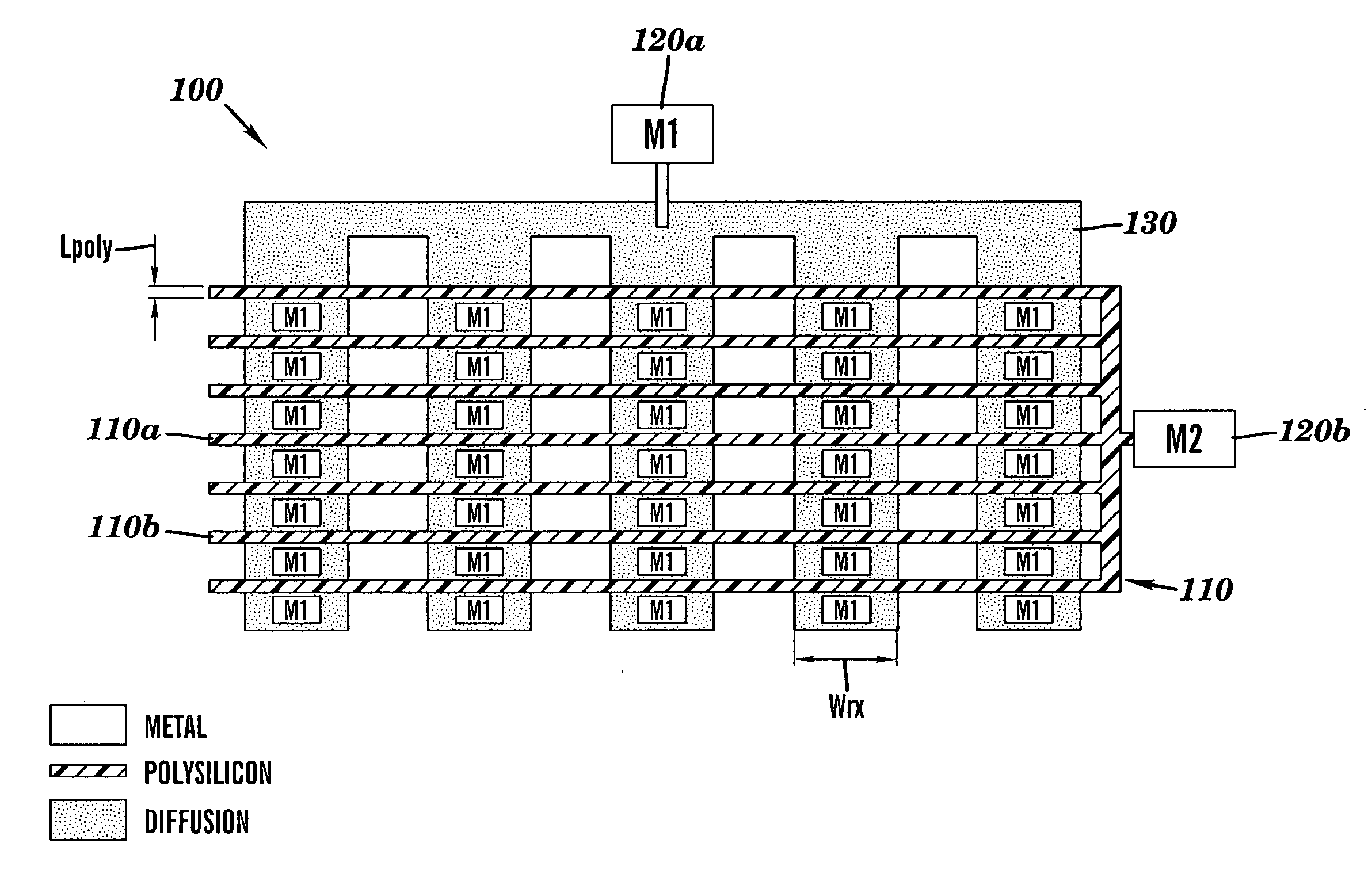
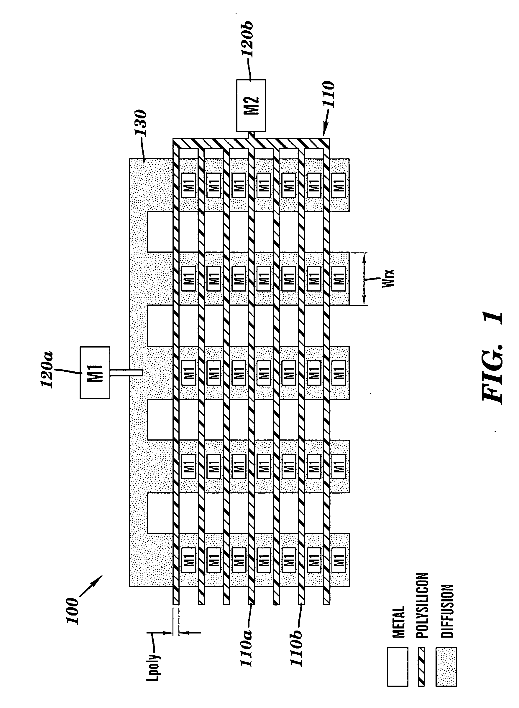
[0008] The present invention is efficient because during manufacturing it detects profile drift in semiconductor wafers in a nondestructive manner that facilitates the generation of profile drift statistics for entire batches of semiconductor wafers. The present invention saves significant costs because the semiconductor wafer is not destroyed or compromised, but instead remains completely intact both during and after testing. In addition, the present invention accurately tests profile drift without requiring a skilled technician to laboriously evaluate individual wafer cross sections under a scanning electron microscope. The present invention facilitates the regular testing of profile drift on a scale much larger than previously possible, which in turn facilitates the generation of a profile drift statistical database with respect to entire lots of semiconductor wafers. The profile drift statistical database streamlines semiconductor wafer fabrication because profile drift can be detected and then corrected much earlier in the semiconductor wafer fabrication process than previously possible.

Problems solved by technology

Over time, however, the ideal, rectangular profile may drift or, in other words, change.
For example, a machine failure in the wafer fabrication plant or a change in process conditions, such as a change in the Reactive Ion Etching (“RIE”) of the PC line, may cause profile drift.
Visual detection is a destructive technique.
Once the wafer has been cut for visual inspection, the wafer cannot be further processed.
Accordingly, visual detection wastes the resource of the wafer as well as needlessly consumes the time of the machines that created the destroyed wafer.
In addition, visual inspection is time consuming for the technician.
Accordingly, the technician does not visually detect each lot or even each bunch of lots.
Because visual detection occurs with so few wafers, statistics cannot accurately be gathered regarding the profile drift of a given lot or even a given bunch of lots.

Method used


Image

  • Structure for monitoring semiconductor polysilicon gate profile
  • Structure for monitoring semiconductor polysilicon gate profile
  • Structure for monitoring semiconductor polysilicon gate profile

Examples


case 2

[0022] Case 2 in FIG. 3 represents an ideal PC profile because the PC profile is rectangular. With an ideal, i.e., rectangular, PC profile, the bottom width of the PC line, L, equals the average width of the cross sectional area of the PC profile, W2. Notice that for case 2, the line that indicates the bottom width of the PC line, L, overlaps the line that indicates the average width of the cross sectional area of the PC profile, W2. PC profile is not always ideal, however, as demonstrated by cases 1 and 3 in FIG. 3. For both cases 1 and 3, the PC profile shape is not rectangular, but instead trapezoidal.

[0023] In case 1, the width of the PC profile is wider at the bottom than at the top of the PC profile. Because the bottom width is wider than the top width, the bottom width will not equal the average width of the cross sectional area. Such is shown in case 1, because the line that indicates the bottom width of the PC profile, L, does not overlap the line that indicates the average...


PUM


Abstract

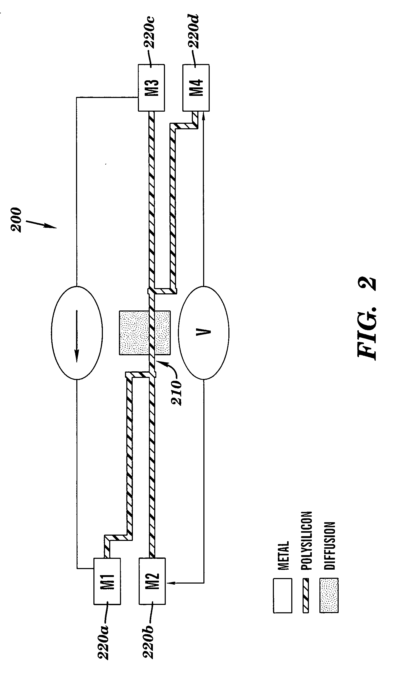
Detection of a profile drift of a polysilicon line is enhanced by a test structure that (1) measures a bottom width and an average width of a cross sectional area of the same polysilicon line (2) correlates the two measurements, and (3) compares such correlation with a previous correlation of bottom width to average width of cross sectional area of the same polysilicon line.

Description

FIELD OF THE INVENTION [0001] The present invention relates generally to semiconductor wafers, and more particularly to polysilicon lines on such semiconductor wafers. BACKGROUND OF THE INVENTION [0002] A semiconductor wafer typically comprises a plurality of polysilicon (“PC”) lines, which transport electrical signals. A cross sectional view taken from the top down of the PC line is known as the profile of the PC line. PC lines have a specific profile in a stable production line. An ideal PC profile is rectangular. Over time, however, the ideal, rectangular profile may drift or, in other words, change. For instance, a PC profile which began as rectangular may drift to trapezoidal in shape. Such drift is known as profile drift. Profile drift may be caused by any number of factors. For example, a machine failure in the wafer fabrication plant or a change in process conditions, such as a change in the Reactive Ion Etching (“RIE”) of the PC line, may cause profile drift. [0003] There i...

Claims


Application Information

Patent Timeline
Patent Type & Authority Applications(United States)
IPC IPC(8): H01L21/66
CPCH01L22/34
Inventor AHSAN, ISHTIAQMACIEJEWSKI, EDWARD P.
Owner IBM CORP
Why Eureka
Try Eureka