Power semiconductor device

a technology of semiconductor devices and semiconductors, applied in the direction of semiconductor devices, basic electric elements, electrical equipment, etc., can solve the problems of low breakdown voltage, complex process steps, and trade-off between device breakdown voltage and breakdown voltag

Inactive Publication Date: 2008-10-09
KK TOSHIBA
View PDF9 Cites 60 Cited by
  • Summary
  • Abstract
  • Description
  • Claims
  • Application Information

AI Technical Summary

Problems solved by technology

Thus there is a tradeoff between the device breakdown voltage and the ON resistance.
However, when more reduction of the ON resistance and more increase of the breakdown voltage of the power semiconductor device using the SJ structure are attempted, the following problems are caused.
As a result, the breakdown voltage becomes low.
However, in this case, process steps get complex, and difficulty of the process turns up.

Method used


Image

  • Power semiconductor device
  • Power semiconductor device
  • Power semiconductor device

Examples


first embodiment

Modified Example of First Embodiment

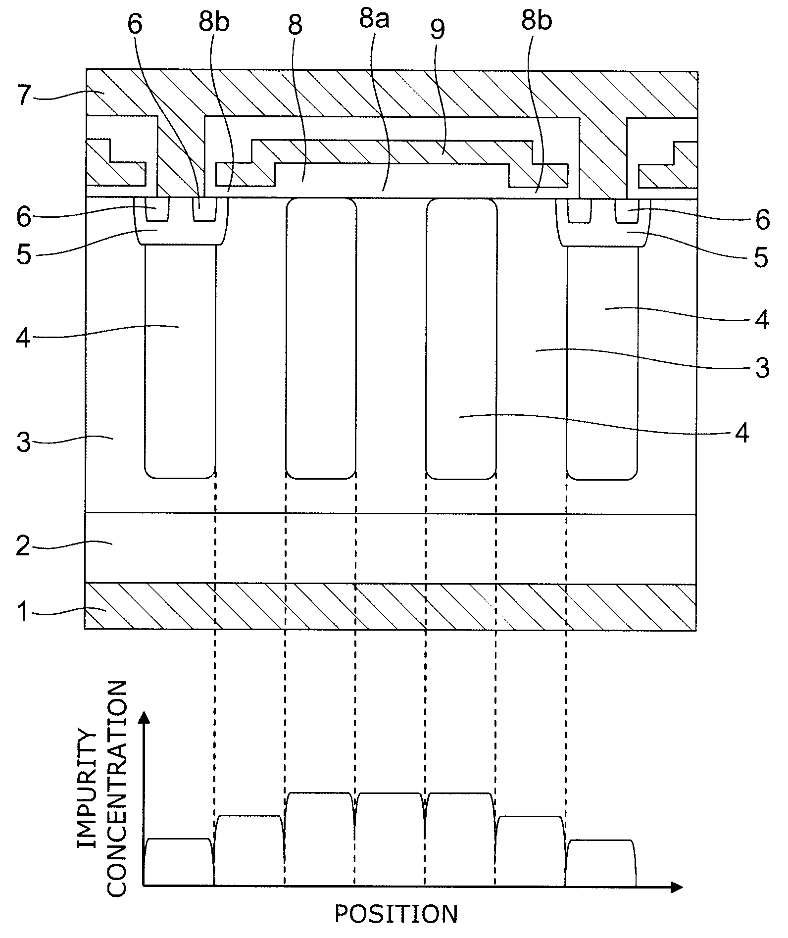
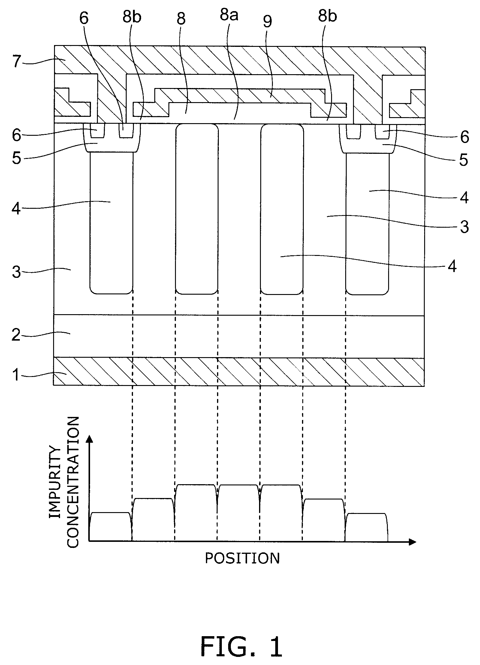
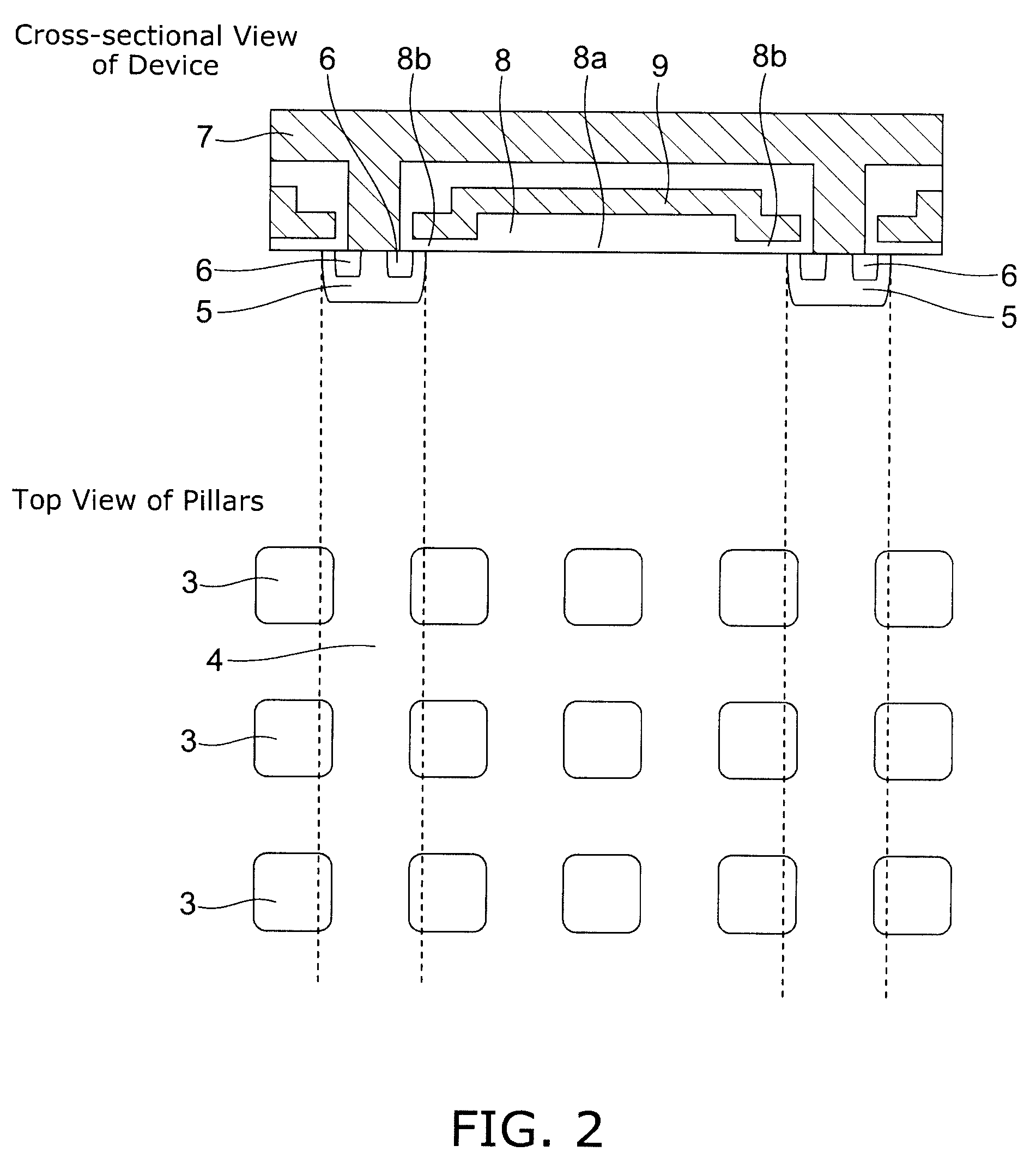
[0044]FIG. 3 is a cross-sectional view schematically illustrating a power MOSFET according to a modified example of the first embodiment and a graphic view illustrating a profile of an impurity concentration of a SJ structure, in which the horizontal axis is position of the lateral direction in the SJ structure and the vertical axis is pillar concentration.

[0045]As shown in FIG. 3, in the power MOSFET according to this modified example, an array period of the p-base layers 5 is large, compared to the power MOSFET according to the above-described first embodiment. Moreover, the peripheral portion of the gate electrode 9 is formed diagonally. More specifically, both end portions of the gate electrode 9 in a longitudinal direction extend in the direction inclining to the upper surface of the n+ drain layer 2. Furthermore, the impurity concentration of each of the pillar layers has an intermediate value of the impurity concentrations of the pillar lay...

second embodiment

[0047]FIG. 4 is a perspective cross-sectional view schematically illustrating a power MOSFET according to a second embodiment of this invention and a graphic view illustrating a profile of an impurity concentration of a SJ structure, in which the horizontal axis is position of the lateral direction in the SJ structure and the vertical axis is pillar concentration.

[0048]As shown in FIG. 4, in the power MOSFET according to this embodiment, the n-pillar layers 3 and the p-pillar layers 4 are formed in a stripe form. Also, the p-base layers 5 are formed in a stripe form and extend along the array direction (lateral direction) of the n-pillar layers 3 and the p-pillar layers 4. That is, the direction to which the p-base layers 5 extend is orthogonal to the direction to which the n-pillar layers 3 and the p-pillar layers 4 extend. Furthermore, the gate electrode 9 is also formed in a stripe form and extends in the direction orthogonal to the direction to which the p-base layers 5 extend, ...

third embodiment

Modified Example of Third Embodiment

[0056]FIG. 6 is a perspective cross-sectional view schematically illustrating a power MOSFET according to a modified example of the third embodiment and a graphic view illustrating a profile of an impurity concentration of a SJ structure, in which the vertical axis is position in the longitudinal direction in the SJ structure and the horizontal axis is pillar concentration.

[0057]As shown in FIG. 6, in the power MOSFET according to this embodiment, the impurity concentration profile of the n-pillar layer 3 and the impurity concentration profile of the p-pillar layer 4 have reverse gradients to each other. That is, along the direction from the source electrode 7 toward the drain electrode 1, the impurity concentration of the p-pillar layer 4 continuously decreases and the impurity concentration of the n-pillar layer 3 continuously increases. Thereby, in a part of the side of the source electrode 7 in the SJ structure, the impurity concentration in t...


PUM


Abstract

A power semiconductor device includes: a first semiconductor layer; a second semiconductor layer and a third semiconductor layer that are provided above the first semiconductor layer and alternatively arranged along a direction parallel to an upper surface of the first semiconductor layer; a plurality of fourth semiconductor layers provided on some of immediately upper regions of the third semiconductor layers and connected to the third semiconductor layer; a fifth semiconductor layer; a control electrode; a gate insulating film; a first main electrode; and a second main electrode. An array period of the fourth semiconductor layers is larger than an array period of the second semiconductor layers. A thickness of a part of the gate insulating film disposed in an immediate upper region of a central portion between the fourth semiconductor layers is thicker than a thickness of a part of the gate insulating film disposed in the immediate upper region of the fourth semiconductor layer. Sheet impurity concentrations of the second semiconductor layer and the third semiconductor layer that are located in the central portion are higher than a sheet impurity concentration of the third semiconductor layer disposed in an immediately lower region of the fourth semiconductor layer.

Description

CROSS-REFERENCE TO RELATED APPLICATIONS[0001]This application is based upon and claims the benefit of priority from the prior Japanese Patent Application No. 2007-097639, filed on Apr. 3, 2007; the entire contents of which are incorporated herein by reference.BACKGROUND OF THE INVENTION[0002]1. Field of the Invention[0003]This invention relates to a power semiconductor device and particularly to a power semiconductor device having a super-junction structure.[0004]2. Background Art[0005]The ON resistance of a vertical power MOSFET (metal-oxide-semiconductor field effect transistor) greatly depends on the electric resistance of its conduction layer (drift layer). The dopant concentration that determines the electric resistance of the drift layer cannot exceed a maximum limit, which depends on the breakdown voltage of a p-n junction between the base layer and the drift layer. Thus there is a tradeoff between the device breakdown voltage and the ON resistance. Improving this tradeoff is...

Claims


Application Information

Patent Timeline
Patent Type & Authority Applications(United States)
IPC IPC(8): H01L29/78
CPCH01L29/0615H01L29/0619H01L29/0634H01L29/0638H01L29/1095H01L29/42368H01L29/7802H01L29/7811H01L29/0878
Inventor SAITO, WATARUONO, SYOTARO
Owner KK TOSHIBA
Why Eureka
Try Eureka