

Semiconductor light emitting device
a technology of semiconductor photodetector and light emitting device, which is applied in the direction of solid-state devices, lasers, semiconductor lasers, etc., can solve the problems of insufficient improvement of light detection precision, effectively suppressed spontaneous emission light to semiconductor photodetector, and achieves the reduction of the spontaneous emission light detection level of semiconductor photodetector, the effect of improving light detection precision
- Summary
- Abstract
- Description
- Claims
- Application Information
AI Technical Summary
Benefits of technology
Problems solved by technology
Method used
Image

Examples
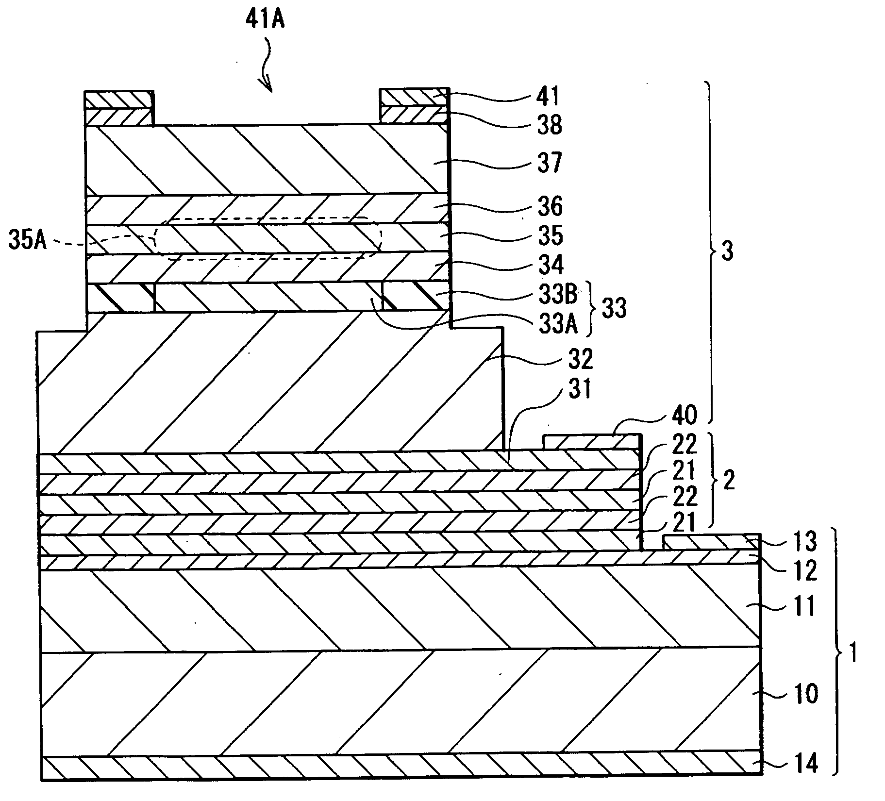
first embodiment
Modification of First Embodiment
[0067]In the foregoing embodiment, the case has been described in which the multilayer filter 2 reflects light having a wavelength shorter than the wavelength λo in the spontaneous emission light L2 included in light output from the VCSEL 3 to the semiconductor photodetector 1 side. The multilayer filter 2 may reflect not only light having a wavelength shorter than the wavelength λo in the spontaneous emission light L2 included in light output from the VCSEL 3 to the semiconductor photodetector 1 side but also light having a wavelength longer than the wavelength λo.
[0068]In this case, it is sufficient to provide the multilayer filter 2 with not only the stack structure obtained by alternately stacking the low-refractive-index layers 21 made of, for example, p-type Alx13Ga1-x13As and each having a thickness of λ1 / 4n5 and the high-refractive-index layers 22 made of, for example, p-type Alx14Ga1-x14As and each having a thickness of λ1 / 4n6 but also, on or...
second embodiment
[0070]FIG. 8 shows the structure of a semiconductor light emitting device as a second embodiment of the present invention. FIG. 8 is a schematic diagram and dimensions and shapes in FIG. 8 are different from actual ones. In the following description, when the same reference numeral as that in the foregoing embodiment is used, it means that the component has the configuration and function similar to those of the component having the same reference numeral. The configurations, operations, and effects different from those of the foregoing embodiment will be mainly described below. Description of configurations, operations, and effects similar to those of the foregoing embodiment will not be repeated.
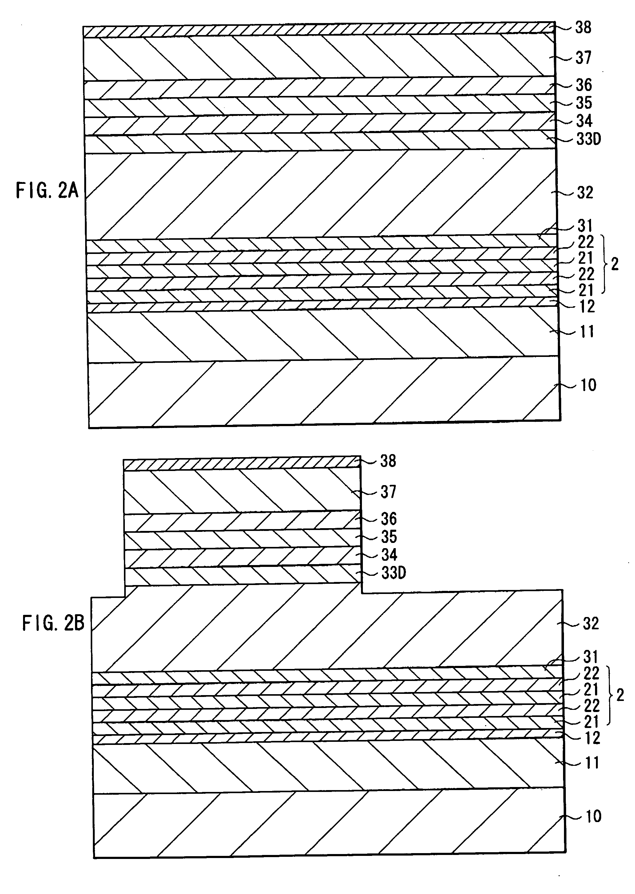
[0071]The semiconductor light emitting device is formed by bonding the multilayer filter 2 formed on one of the semiconductor photodetector 1 and the VCSEL 3 to the other one on which the multilayer filter 2 is not formed.
[0072]The semiconductor light emitting device is obtained by stacking...
PUM
 Abstract
Description
Claims
Application Information