Chip stack package and method of fabricating the same

Active Publication Date: 2008-10-16
SAMSUNG ELECTRONICS CO LTD
View PDF3 Cites 25 Cited by
  • Summary
  • Abstract
  • Description
  • Claims
  • Application Information

AI Technical Summary

Benefits of technology

[0011]The present invention provides a chip stack package, wherein semiconductor chips having different sizes are stacked by arranging pads in a scr

Problems solved by technology

However, such methods cause warpage of the package or make the package difficult to handle in processing step

Method used


Image

  • Chip stack package and method of fabricating the same
  • Chip stack package and method of fabricating the same
  • Chip stack package and method of fabricating the same

Examples


Embodiment Construction

[0022]The present invention will now be described more fully hereinafter with reference to the accompanying drawings, in which preferred embodiments of the invention are shown. This invention may, however, be embodied in many different forms, and should not be construed as being limited to the embodiments set forth herein. Rather, these embodiments are provided so that this disclosure will be thorough and complete, and will fully convey the scope of the invention to those skilled in the art. In the drawings, the thicknesses of layers and regions are exaggerated for clarity. Like numbers refer to like elements throughout the specification.

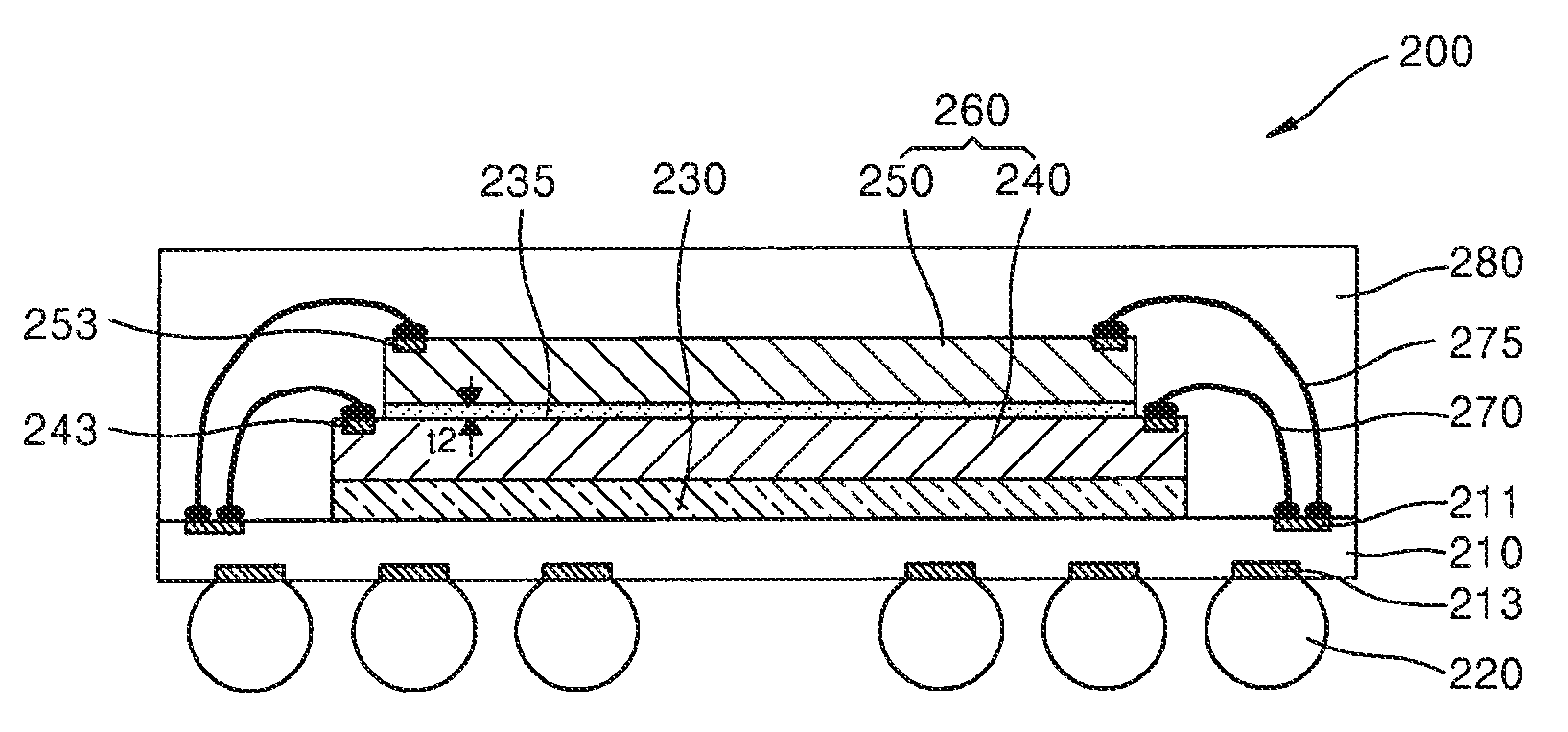
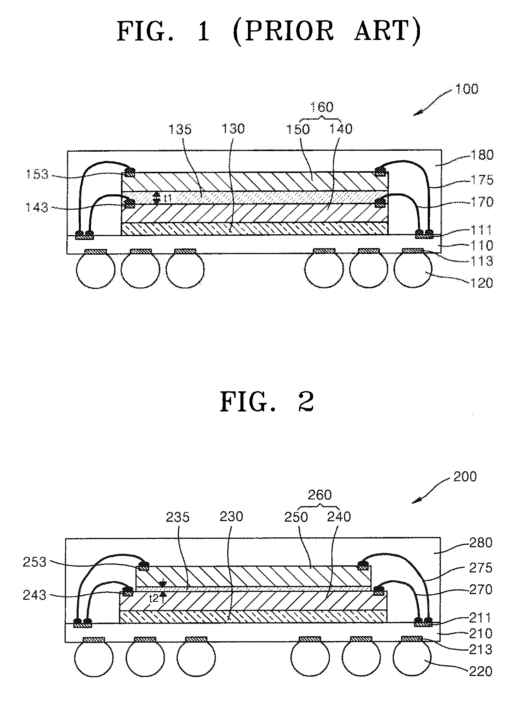
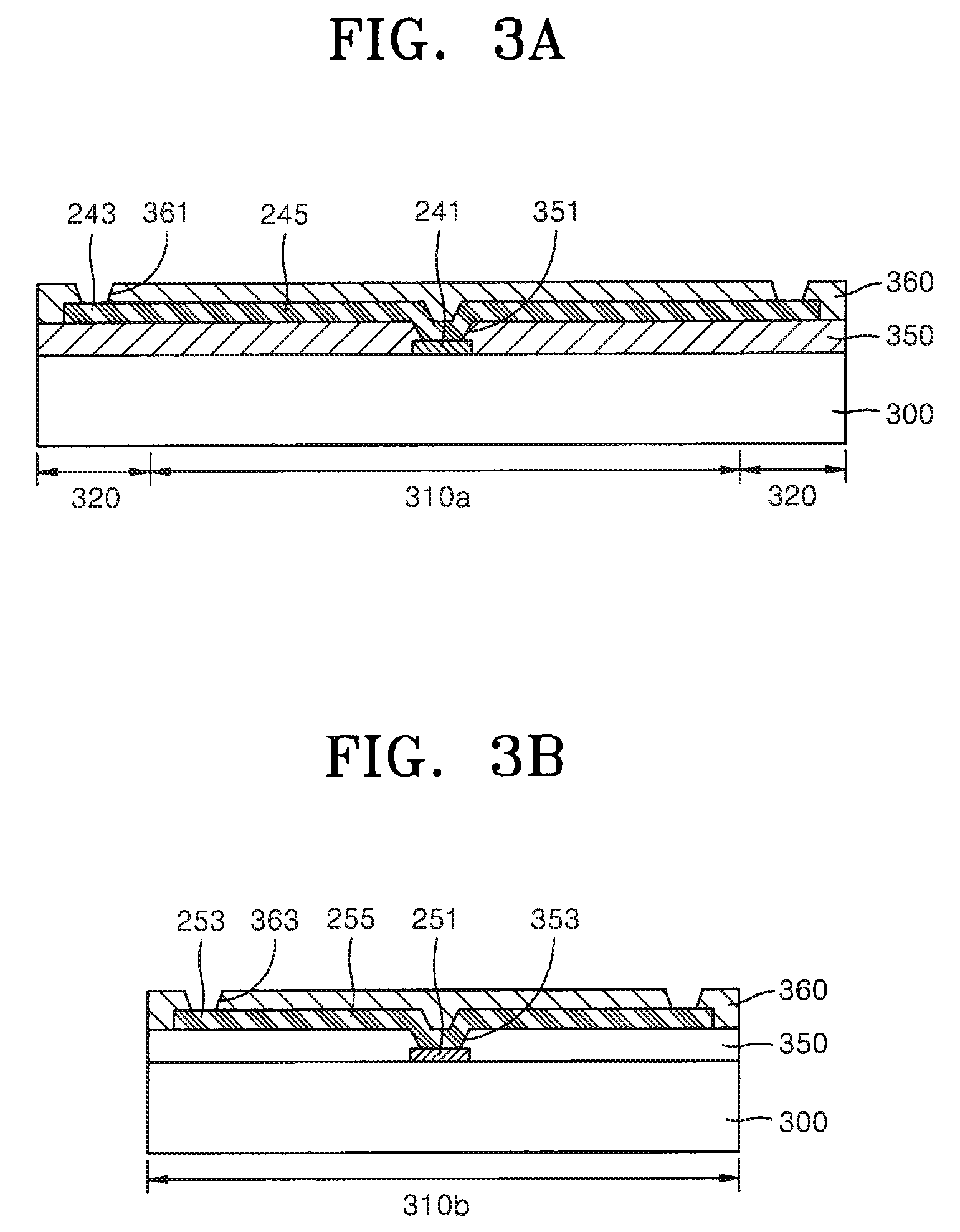
[0023]FIG. 2 is a cross-sectional view of a chip stack package according to an embodiment of the present invention. FIGS. 3A and 3B are cross-sectional views of first and second semiconductor chips, respectively, in the chip stack package of FIG. 2. Referring to FIGS. 2, 3A and 3B, the chip stack package 200 includes a substrate 210 and a unit semic...


PUM


Abstract

A chip stack package is provided, wherein semiconductor chips having different die sizes are stacked by arranging pads in a scribe region through a redistribution process, so that the thickness of the package can be reduced. A method of fabricating the chip stack package is also provided. In the chip stack package, a plurality of circuit patterns are arranged on one surface of a substrate, and a unit semiconductor chip is mounted thereon. The unit semiconductor chip includes a plurality of semiconductor chips sequentially stacked on the substrate. The semiconductor chips of the unit semiconductor chip have different die sizes. One of the semiconductor chips includes a plurality of first pads arranged in a first chip region, and the other semiconductor chips include second pads arranged in a scribe region at an outside of a second chip region defined by the scribe region.

Description

CROSS-REFERENCE TO RELATED PATENT APPLICATION[0001]This application claims priority under 35 USC §119 to Korean Patent Application No. 10-2007-0035176, filed on Apr. 10, 2007 in the Korean Intellectual Property Office, the disclosure of which is incorporated herein in its entirety by reference.BACKGROUND[0002]1. Technical Field[0003]This disclosure relates to a semiconductor package, and more particularly, to a chip stack package having a reduced thickness, and a method of fabricating the chip stack package.[0004]2. Description of the Related Art[0005]As electronic devices, such as portable personal computers (PCs) and mobile telephones, get smaller and become multifunctional, by virtue of the rapid development of digital technology, they need smaller, lighter and higher capacity semiconductor devices. The integration density of a semiconductor device increases with the capacity of a semiconductor package. To achieve very high integration density, a stack package contains a pluralit...

Claims


Application Information

Patent Timeline
IPC IPC(8): H01L23/498
CPCH01L23/3128H01L23/525H01L25/0657H01L2224/32145H01L2224/48091H01L2224/48227H01L2224/73265H01L2225/0651H01L2225/06517H01L2225/06527H01L2924/15311H01L2924/00014H01L24/48H01L2924/01322H01L2224/45139H01L2924/00H01L2224/32225H01L2924/00012H01L24/45H01L24/73H01L2924/181H01L2224/05554H01L2924/10161H01L2924/00011H01L2224/45099H01L2924/01049H01L2224/45015H01L2924/207H01L23/12
Inventor CHUNG, HYUN-SOOLEE, DONG-HOKIM, NAM-SEOGHWANG, SON-KWAN
Owner SAMSUNG ELECTRONICS CO LTD
Why Eureka
Try Eureka