Probe for testing semiconductor devices

a technology for semiconductor devices and contactors, applied in the direction of electrical testing, measurement devices, instruments, etc., can solve the problems of increasing the cost of probe cards, requiring a larger probe force, and affecting the reliability of probe cards, so as to improve the tolerance of fracture failure and reduce stress

Active Publication Date: 2008-10-16
FORMFACTOR INC
View PDF5 Cites 7 Cited by
  • Summary
  • Abstract
  • Description
  • Claims
  • Application Information

AI Technical Summary

Benefits of technology

[0015]All three embodiments may be used together or in any combination, to achieve better stress reduction and increased tolerance to fracture failures. Also, all three embodiments may be used in a hybrid probe design, or a pure torsional design.

Problems solved by technology

This results in a larger tip contact area and a larger probe force is thus needed to pierce the aluminum oxide layer.
When you multiply this force by the hundreds or thousands of probes on a probe card, the probe card must be engineered to accommodate significant forces, which usually means reinforcing the probe card components, which in turn increases probe card costs.
It is clear from FIGS. 8A and 8B that the stress distribution is inefficient because only small portions of the bending element absorb the stress.
And it is in these small portions where the probe is more likely to fail forcing manufacturers to widen the bending element at the probe foot to reduce stress and prevent failures.
A wider bending element near the probe base, however, adversely affects the packing density of the probe card.
This results in a smaller tip contact area and a smaller probe force is thus needed to pierce the aluminum oxide layer, which in turn, reduces the overall force exerted by the probe card.
Unfortunately though, the torsional probe too has drawbacks.
First, for a typical torsional design with a shorter geometry of the arm, the scrub length is generally longer which can limit the size of contact pads for the DUTs.
This z-deformation may be caused by material fatigue.
And third, at the union angle (where the torsional member meets a second element of the probe) there can be significant stress which can cause fractures, and thus, render the probe inoperable.

Method used


Image

  • Probe for testing semiconductor devices
  • Probe for testing semiconductor devices
  • Probe for testing semiconductor devices

Examples


Embodiment Construction

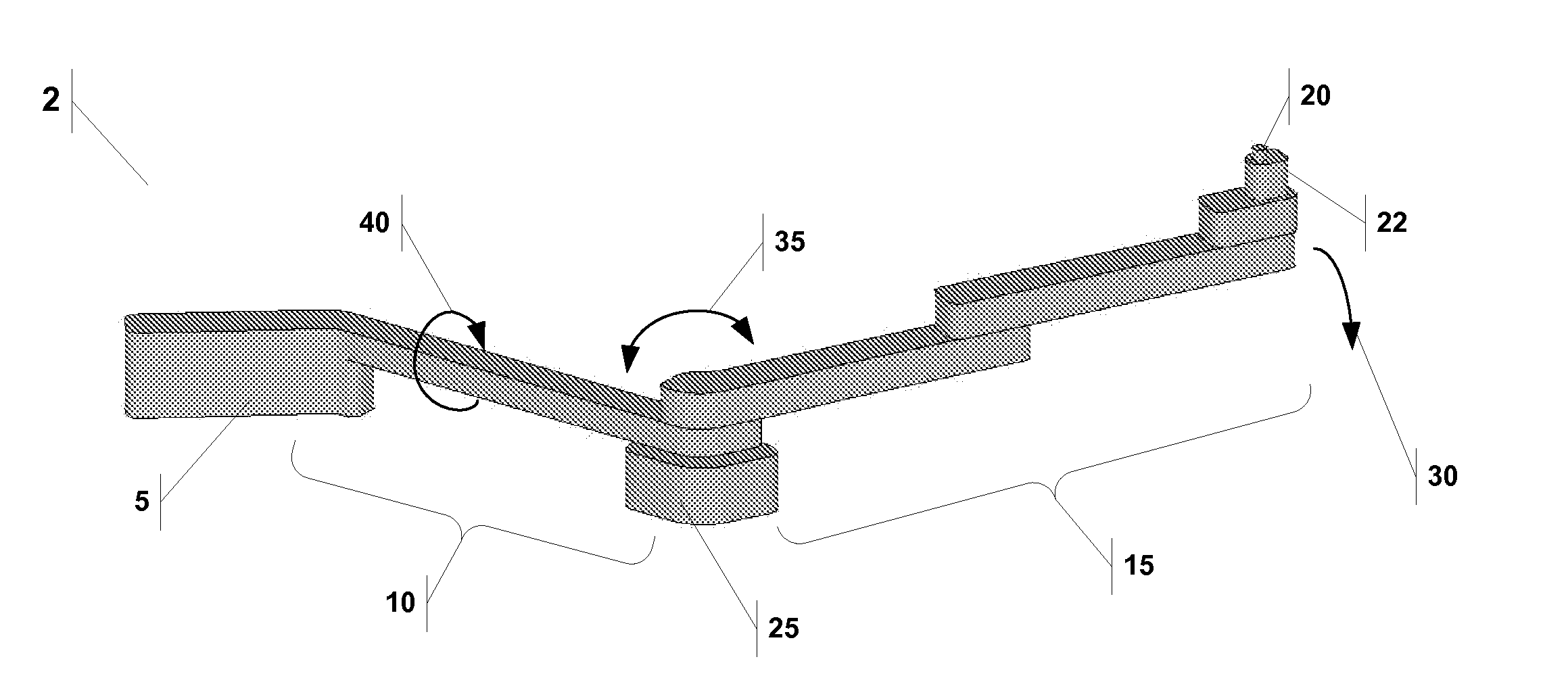
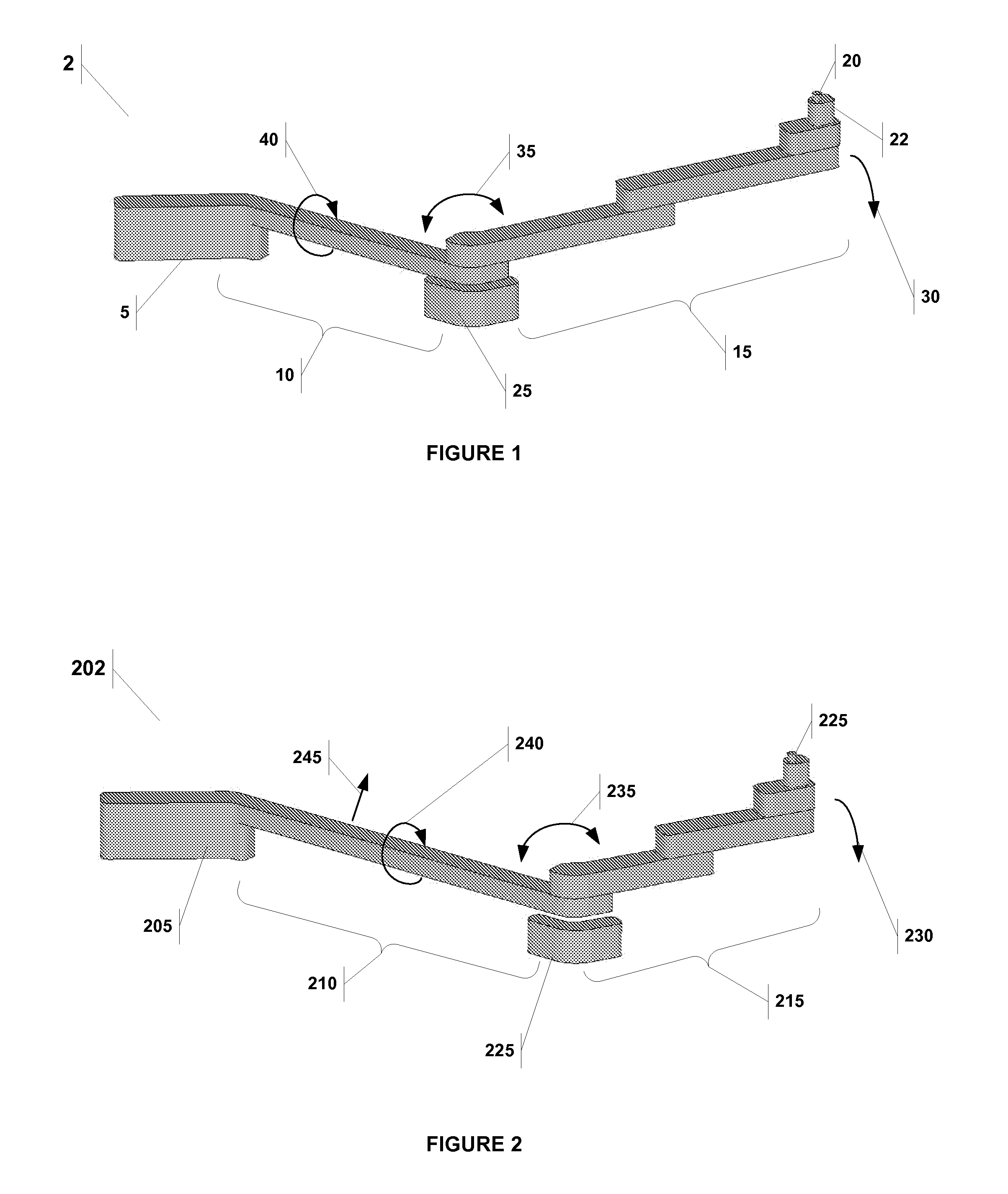
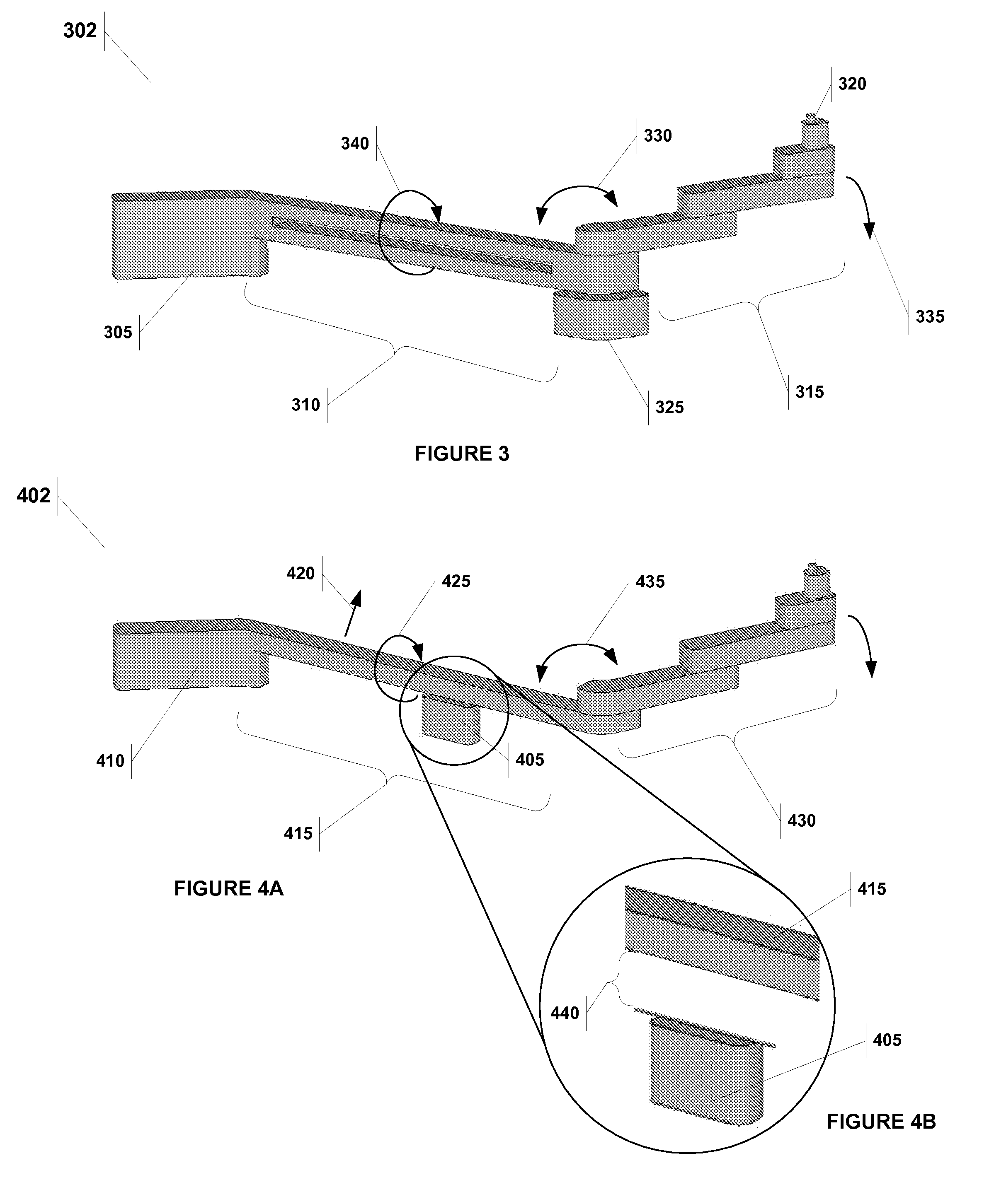
[0033]What is described below is a novel hybrid probe design that comprises a torsion element and a bending element. Also described below are novel probe designs that incorporate various union angle interface edge shapes, pivot cutouts and buffer layers to prevent failure from stress fractures.

[0034]Turning first to the hybrid probe, both the torsion and bending elements allow the hybrid probe to store the displacement energy through torsion and bending. The hybrid design exploits the advantages of both the torsional and cantilever probe designs (i.e., greater packing density, less probe failure from material fatigue, less probe card force, and shorter scrub lengths), while minimizing the disadvantages of a non-hybrid design. The hybrid design can be used to manufacture a probe card that is optimized to a particular application, further increasing the probe card efficiency and cost effectiveness.

[0035]FIG. 1 presents an embodiment of a novel hybrid probe (2). The hybrid probe (2) co...


PUM


Abstract

A novel probe design is presented that increases a probe tolerance to stress fractures. Specifically, what is disclosed are three features increase stress tolerance. These features include a various union angle interface edge shapes, pivot cutouts and buffers.

Description

1. FIELD OF THE INVENTION[0001]The present invention relates to devices for testing semiconductor devices and more particularly to the design of probe contactors for such testing.2. BACKGROUND OF THE INVENTION[0002]Integrated circuits are made in a bulk parallel process by patterning and processing semiconductor wafers. Each wafer contains many identical copies of the same integrated circuit referred to as a “die.” It may be preferable to test the semiconductor wafers before the die is cut into individual integrated circuits and packaged for sale. If defects are detected the defective die can be culled before wasting resources packaging a defective part. The individual die can also be tested after they have been cut into individual integrated circuits and packaged.[0003]To test a wafer or an individual die—commonly called the device under test or DUT—a probe card is commonly used which comes into contact with the surface of the DUT. The probe card generally contains three unique cha...

Claims


Application Information

Patent Timeline
Patent Type & Authority Applications(United States)
IPC IPC(8): G01R1/067
CPCG01R1/06727G01R1/06733
Inventor AN, ZHIYONGKHOO, MELVINTEA, NIMHU, TING
Owner FORMFACTOR INC
Why Eureka
Try Eureka