Receiving apparatus and signal processing method

a technology of receiving apparatus and signal processing method, which is applied in the direction of multiplex communication, orthogonal multiplex, pulse technique, etc., can solve the problems of increasing the number of required bits for the adc, difficult to remove the dc offset within such a short switching time, and deteriorating signals, so as to reduce the increase in circuit size and remove the dc offset. reliably

Inactive Publication Date: 2008-10-16
RENESAS ELECTRONICS CORP
View PDF13 Cites 15 Cited by
  • Summary
  • Abstract
  • Description
  • Claims
  • Application Information

AI Technical Summary

Benefits of technology

[0021]The technique of the present invention reliably removes DC offset of a demodulator, while suppressing an increase in circuit size, when receiving a communication signal with frequency hopping among a plurality of frequency bands.

Problems solved by technology

The DC offset is superimposed on a baseband signal to enlarge the voltage amplitude width of the signal, which causes signal distortion to occur due to saturation in the low-pass filter or the amplifier in the subsequent stage, leading to signal degradation.
Further, if the voltage amplitude width of the signal which is input to an analog-to-digital converter (ADC) in an input unit of the baseband processing circuit 8 increases because of the above-described enlargement of the signal voltage amplitude width, it becomes problematic because it leads increase of the number of required bits for the ADC.
It is difficult to remove DC offset within such a short switching time.
For example, according to the technique disclosed in Japanese Unexamined Patent Application Publication No. 2004-172693 (Ono et al), the DC offset correction takes 20 μs, and it is thus incapable of performing high-speed DC offset correction, which is required when receiving a communication signal in the MB-OFDM communication system.
Further, the technique requires a circuit and a sequence for adjusting IDAC, which causes an increase in circuit size.

Method used


Image

  • Receiving apparatus and signal processing method
  • Receiving apparatus and signal processing method
  • Receiving apparatus and signal processing method

Examples


first embodiment

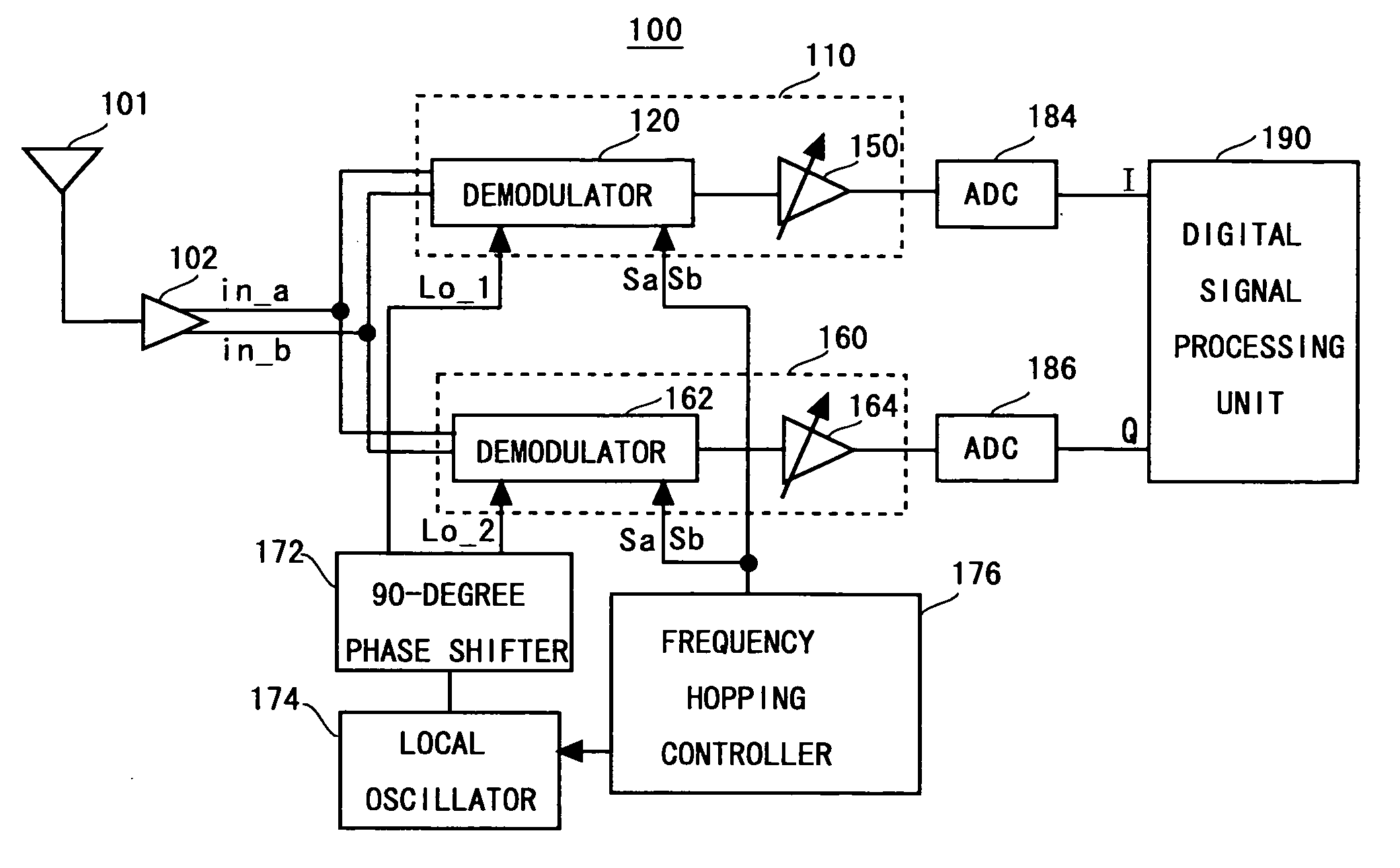
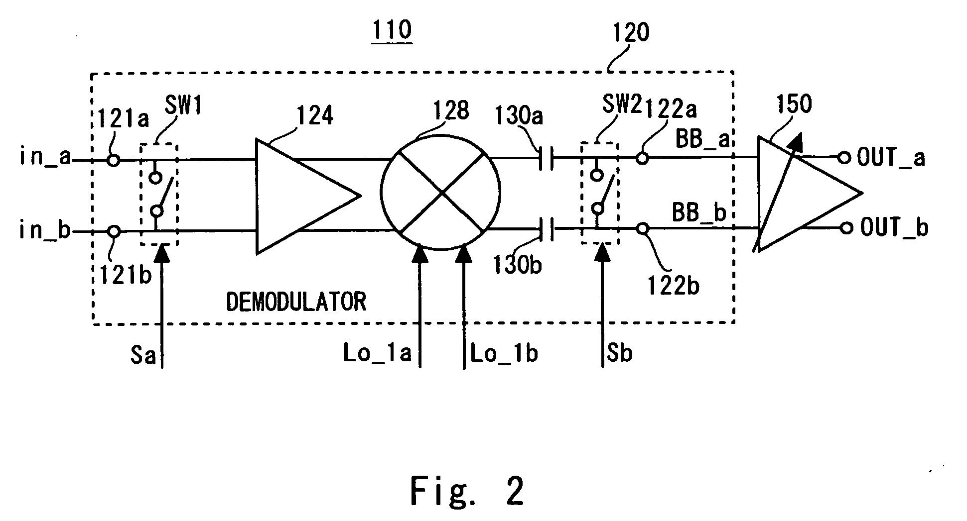
[0036]FIG. 1 shows a receiving apparatus 100 according to a first embodiment of the present invention. The receiving apparatus 100 is such that a receiving apparatus according to the present invention is applied to a receiving side of the MB-OFDM communication system, and it is a radio receiving apparatus of direct-conversion type. As shown in FIG. 1, the receiving apparatus 100 includes an antenna 101 that acquires a communication signal (RF signal), a low noise amplifier 102 that amplifies the RF signal which is acquired by the antenna 101 and converts the signal into differential signals in_a and in_b. The receiving apparatus 100 also includes a first processing circuit 110 that obtain an I-axis signal from the differential signals in_a and in_b, an ADC 184, a second processing circuit 160 that obtain a Q-axis signal from the differential signals in_a and in_b, an ADC 186, and a digital signal processing unit 190 that performs signal processing in a subsequent stage to the ADC 18...

second embodiment

[0057]According to the first embodiment of the present invention shown in FIG. 1, the output terminals 122a and 122b of the demodulator 120 are short-circuited by the switch SW2 in synchronization with frequency switching of a local signal, thereby accumulating changes in DC offset due to frequency hopping in the capacitors 130a and 130b so as to substantially eliminate a voltage difference between the output terminals 122a and 122b. Another technique may be used as long as the changes in DC offset due to frequency hopping can be accumulated in the capacitors 130a and 130b during the guard interval period so that a voltage difference between the output terminals 122a and 122b is substantially eliminated. As a second embodiment, another demodulator which may be used in the receiving apparatus 100 is described hereinafter with reference to FIG. 4.

[0058]FIG. 4 shows a demodulator 140. In the followings, only differences between the demodulator 140 and the demodulator 120 are described,...

third embodiment

[0063]FIG. 5 shows a receiving apparatus 200 according to a third embodiment of the present invention. The receiving apparatus 200 is also a receiving apparatus in the MB-OFDM communication system, and it has a functional block having the same function as each element of the receiving apparatus 100 shown in FIG. 1. In the receiving apparatus 200, a first processing circuit 210 and a second processing circuit 260 are different from the first processing circuit 110 and the second processing circuit 160 in the receiving apparatus 100. The other elements are the same as equivalent elements in the receiving apparatus 100, and they are denoted by the same reference symbols as in the receiving apparatus 100 and not described in detail herein.

[0064]The first processing circuit 210 and the second processing circuit 260 have the same configuration and function except that the phases of input local signals are different by 90 degrees. Thus, only the first processing circuit 210 is described he...


PUM


Abstract

In the reception and demodulation of a communication signal with frequency hopping among a plurality of frequency bands, a demodulator is formed by a balance circuit. The demodulator performs frequency conversion by multiplying signals in_a and in_b, which are obtained by converting a received signal into differential signals, by local signals Lo—1a and Lo—1b with a frequency corresponding to a frequency band of the received signal, which are frequency-switched during a guard interval period of the received signal, in synchronization with a symbol of the received signal. Further, two output ends of the demodulator are charged / discharged through capacitors in synchronization with frequency switching of the local signal so that a voltage difference between the two output ends of the demodulator becomes a prescribed level.

Description

BACKGROUND OF THE INVENTION[0001]1. Field of the Invention[0002]The present invention relates to a radio receiving apparatus and, particularly, to a technique of receiving a frequency-hopping communication signal.[0003]2. Description of Related Art[0004]In the field of radio communication, a multicarrier transmission system is in the limelight as a technique of suppressing the effect of frequency selective fading. Because the multicarrier transmission system transmits data by dividing it into a plurality of carries with different frequencies, the frequency band of each carrier is narrow, so that it is less subject to the effect of frequency selective fading.[0005]For example, in the orthogonal frequency-division multiplexing (OFDM), which is one of the multicarrier transmission system, the frequency of each carrier is set so that the carriers are orthogonal to each other within a symbol space. When transmitting data, the system performs the serial-to-parallel conversion of a serial ...

Claims


Application Information

Patent Timeline
Patent Type & Authority Applications(United States)
IPC IPC(8): H04B1/00H04B1/713H04B1/7156H04J11/00
CPCH04B1/30H04B1/7136H04B2001/71365H04L25/062H04L27/2602
Inventor OHBA, HIDEO
Owner RENESAS ELECTRONICS CORP
Why Eureka
Try Eureka