4f2 self align side wall active phase change memory

a phase change memory and side wall technology, applied in semiconductor devices, digital storage, instruments, etc., can solve problems such as problems in manufacturing such devices with very small dimensions

Active Publication Date: 2008-10-23
MACRONIX INT CO LTD
View PDF92 Cites 58 Cited by
  • Summary
  • Abstract
  • Description
  • Claims
  • Application Information

AI Technical Summary

Problems solved by technology

Problems have arisen in manufacturing such devices with very small dimensions, and with variations in process that meet tight specifications needed for large-scale memory devices.

Method used


Image

  • 4f2 self align side wall active phase change memory
  • 4f2 self align side wall active phase change memory
  • 4f2 self align side wall active phase change memory

Examples


Embodiment Construction

[0024]The following description of the invention will typically be with reference to specific structural embodiments and methods. It is to understood that there is no intention to limit the invention to the specifically disclosed embodiments and methods but that the invention may be practiced using other features, elements, methods, and embodiments. Preferred embodiments are described to illustrate the present invention, not to limit its scope, which is defined by the claims. Those of ordinary skill in the art will recognize a variety of equivalent variations on the description that follows. Like elements in various embodiments are commonly referred to with like reference numerals.

[0025]A detailed description is provided with reference to FIGS. 1-25.

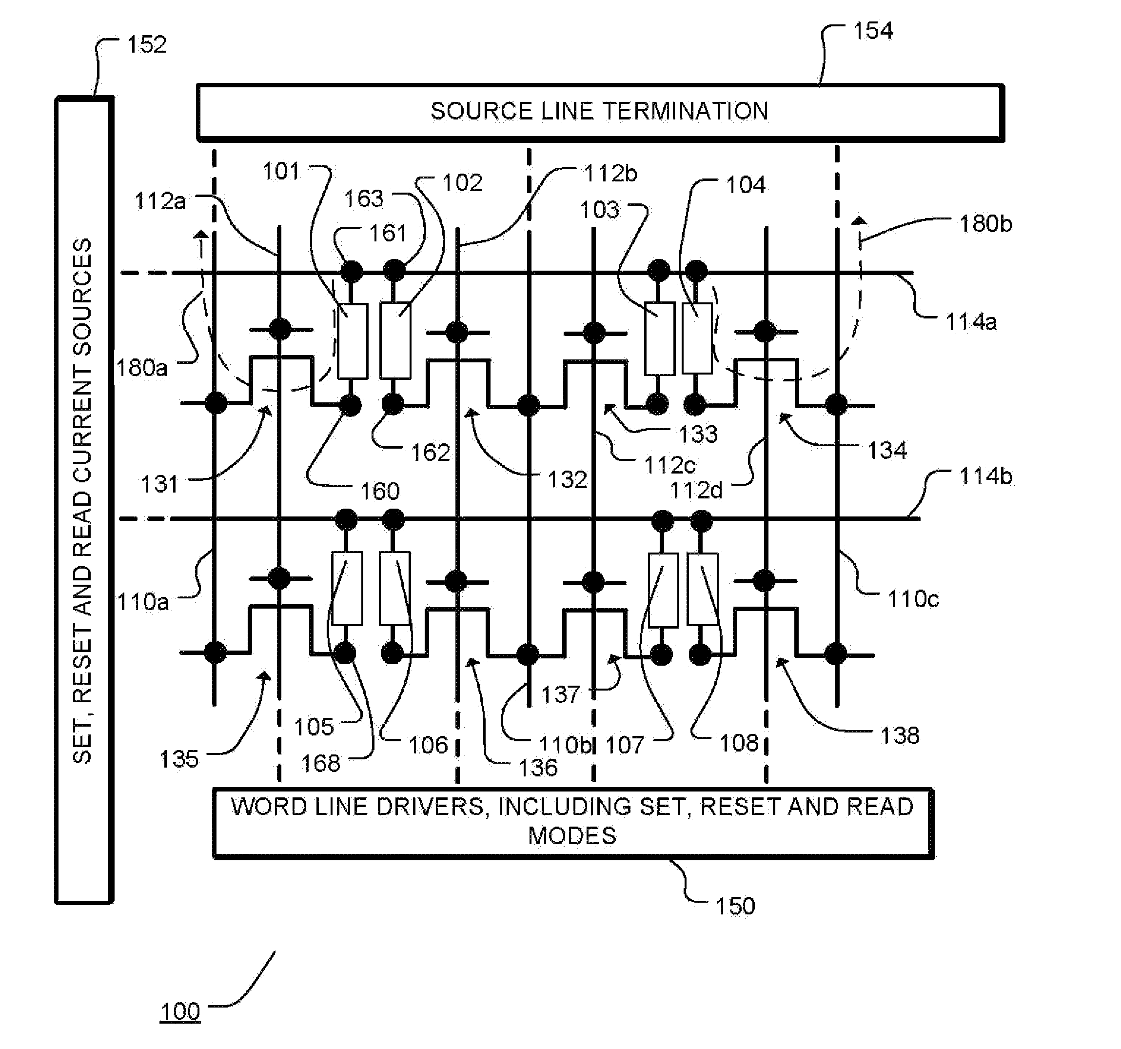
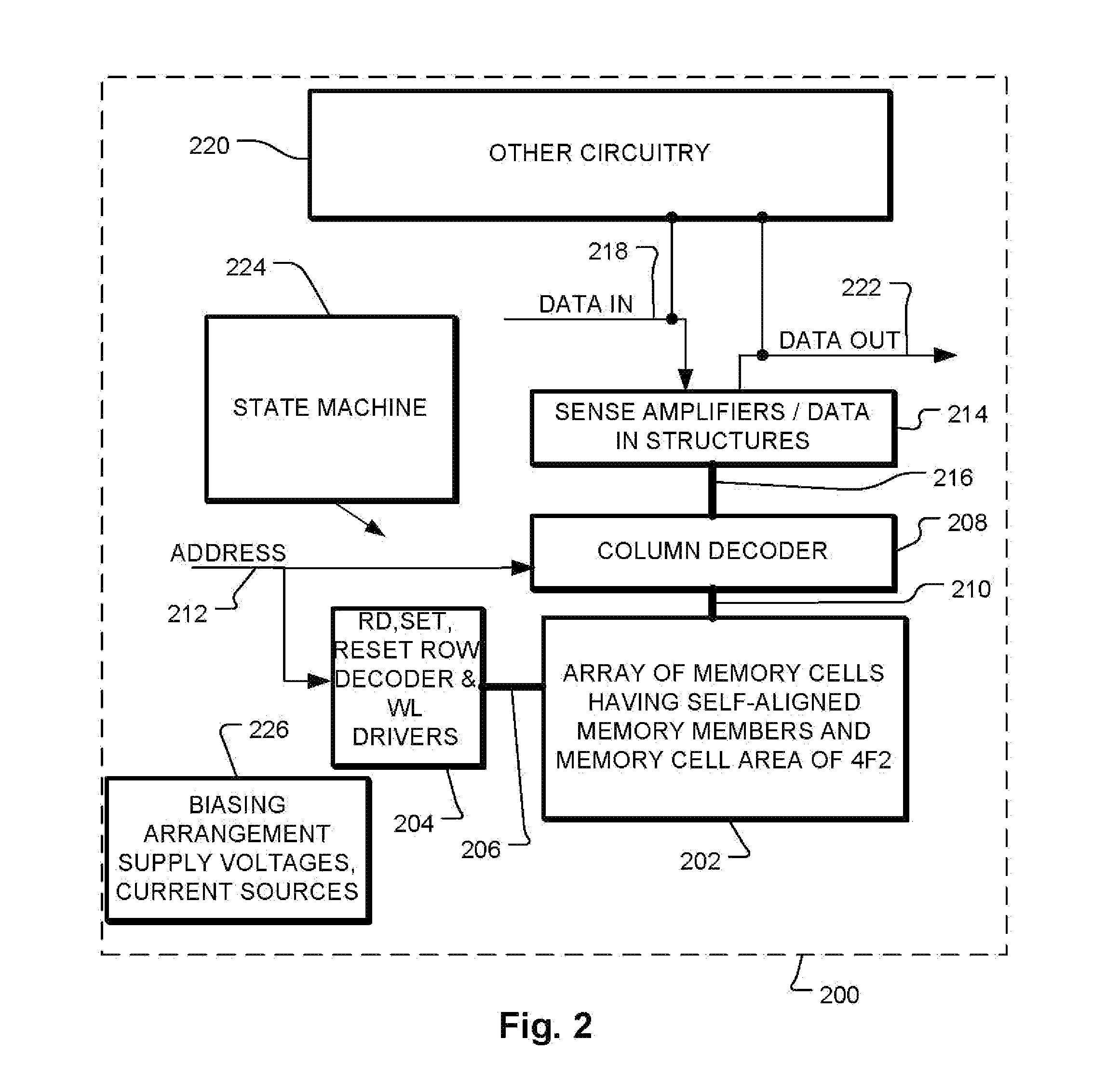
[0026]FIG. 1 is a schematic illustration of a memory array 100, which can be implemented using memory cells as described with reference to FIG. 3, or with other memory cells as described herein. Eight memory cells 131, 132, 133, 134, 135...


PUM


Abstract

Arrays of memory cells are described along with devices thereof and method for manufacturing. Memory cells described herein include self-aligned side wall memory members comprising an active programmable resistive material. In preferred embodiments the area of the memory cell is 4F2, F being the feature size for a lithographic process used to manufacture the memory cell, and more preferably F being equal to a minimum feature size. Arrays of memory cells described herein include memory cells arranged in a cross point array, the array having a plurality of word lines and source lines arranged in parallel in a first direction and having a plurality of bit lines arranged in parallel in a second direction perpendicular to the first direction.

Description

PARTIES TO A JOINT RESEARCH AGREEMENT[0001]International Business Machines Corporation, a New York corporation; Macronix International Corporation, a Taiwan corporation, and Infineon Technologies A.G., a German corporation, are parties to a Joint Research Agreement.BACKGROUND OF THE INVENTION[0002]1. Field of the Invention[0003]The present invention relates to high density memory devices based on phase change based memory materials, including chalcogenide based materials and on other programmable resistive materials, and to methods for manufacturing such devices.[0004]2. Description of Related Art[0005]Phase change based memory materials are widely used in read-write optical disks. These materials have at least two solid phases, including for example a generally amorphous solid phase and a generally crystalline solid phase. Laser pulses are used in read-write optical disks to switch between phases and to read the optical properties of the material after the phase change.[0006]Phase ...

Claims


Application Information

Patent Timeline
Patent Type & Authority Applications(United States)
IPC IPC(8): G11C11/00H01L45/00
CPCB82Y10/00G11C11/5664G11C11/5678G11C11/5685G11C13/0004G11C13/0007G11C13/0014G11C13/0016G11C2213/31G11C2213/32G11C2213/79H01L27/2436H01L27/2463H01L45/04H01L45/06H01L45/124H01L45/14H01L45/144H01L45/146H01L45/147H01L45/1625H01L45/1641H01L45/1691H10B63/30H10B63/80H10N70/8265H10N70/231H10N70/20H10N70/881H10N70/8836H10N70/8828H10N70/8833H10N70/041H10N70/068H10N70/026
Inventor LUNG, HSIANG LAN
Owner MACRONIX INT CO LTD
Why Eureka
Try Eureka