Active device array substrate

a technology of active devices and array substrates, which is applied in static indicating devices, instruments, non-linear optics, etc., can solve the problems of increased number of pixels controlled by each scan line on the active device array substrate, line defect, and exaggerated gate delay effect in each scan line, so as to reduce the gate delay effect and prevent damage , the effect of improving the display quality of the lcd

Active Publication Date: 2008-10-30
AU OPTRONICS CORP
View PDF7 Cites 10 Cited by
  • Summary
  • Abstract
  • Description
  • Claims
  • Application Information

AI Technical Summary

Benefits of technology

[0010]In view of the foregoing conventional issues, the present invention is directed to an active device array substrate capable of improving gate delay defects.
[0022]Based on the above, the present invention is able to reduce the gate delay effect occurring in the active device array substrate through disposing the voltage pull-down circuit. Moreover, the voltage pull-down circuit of the present invention is equipped with a function of electrostatic discharge protection, such that the voltage pull-down circuit can be prevented from damaging due to electrostatic discharge. Therefore, the display quality of the LCD is improved.

Problems solved by technology

However, with an increasing demand on large-size and high-resolution TFT-LCDs, the number of the pixels controlled by each of the scan lines on the active device array substrate is increased, such that gate delay effect occurring in each of the scan lines is exaggerated.
However, during a process of fabricating the LCD, as the voltage pull-down circuit is damaged by electrostatic discharge (e.g. charges generated by a plasma which is used in a thin film deposition or a dry etching, the charges generated by an alignment rubbing process, or the charges generated from conducting a charge test on a substrate), the voltage pull-down circuit may not function, leading to occurrence of line defect.

Method used


Image

  • Active device array substrate
  • Active device array substrate
  • Active device array substrate

Examples


Embodiment Construction

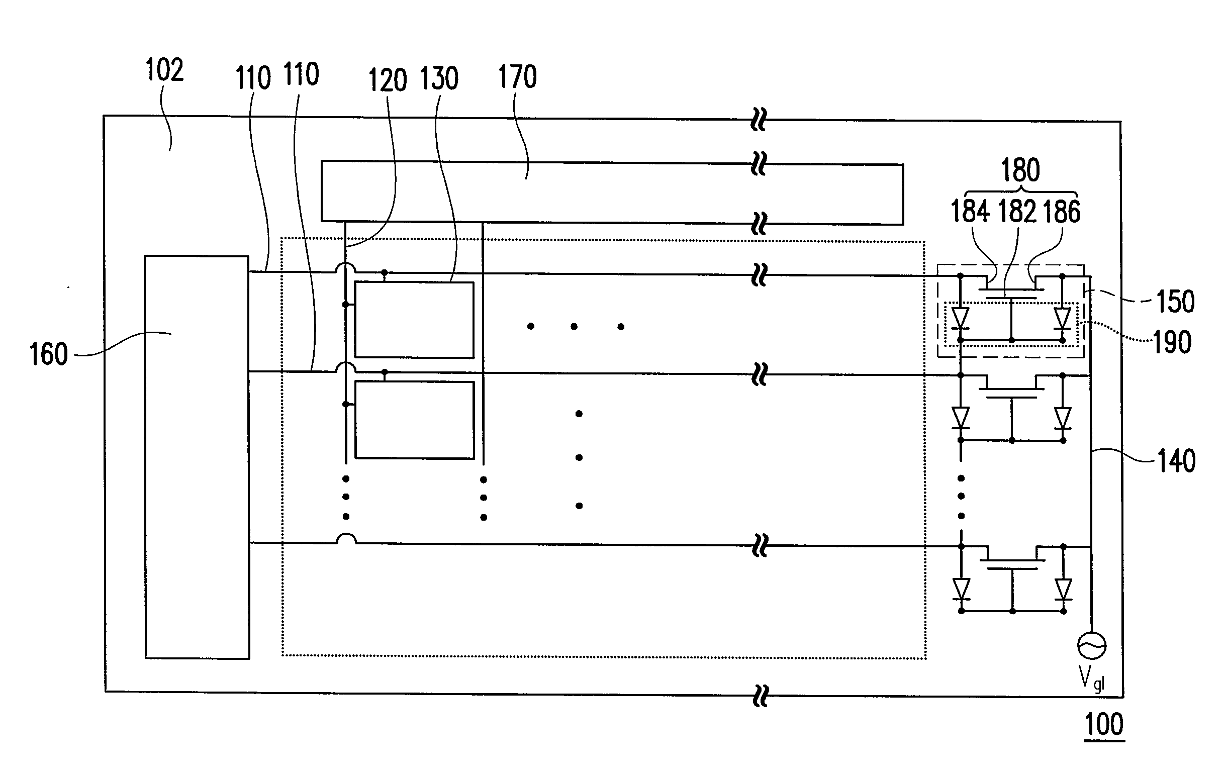
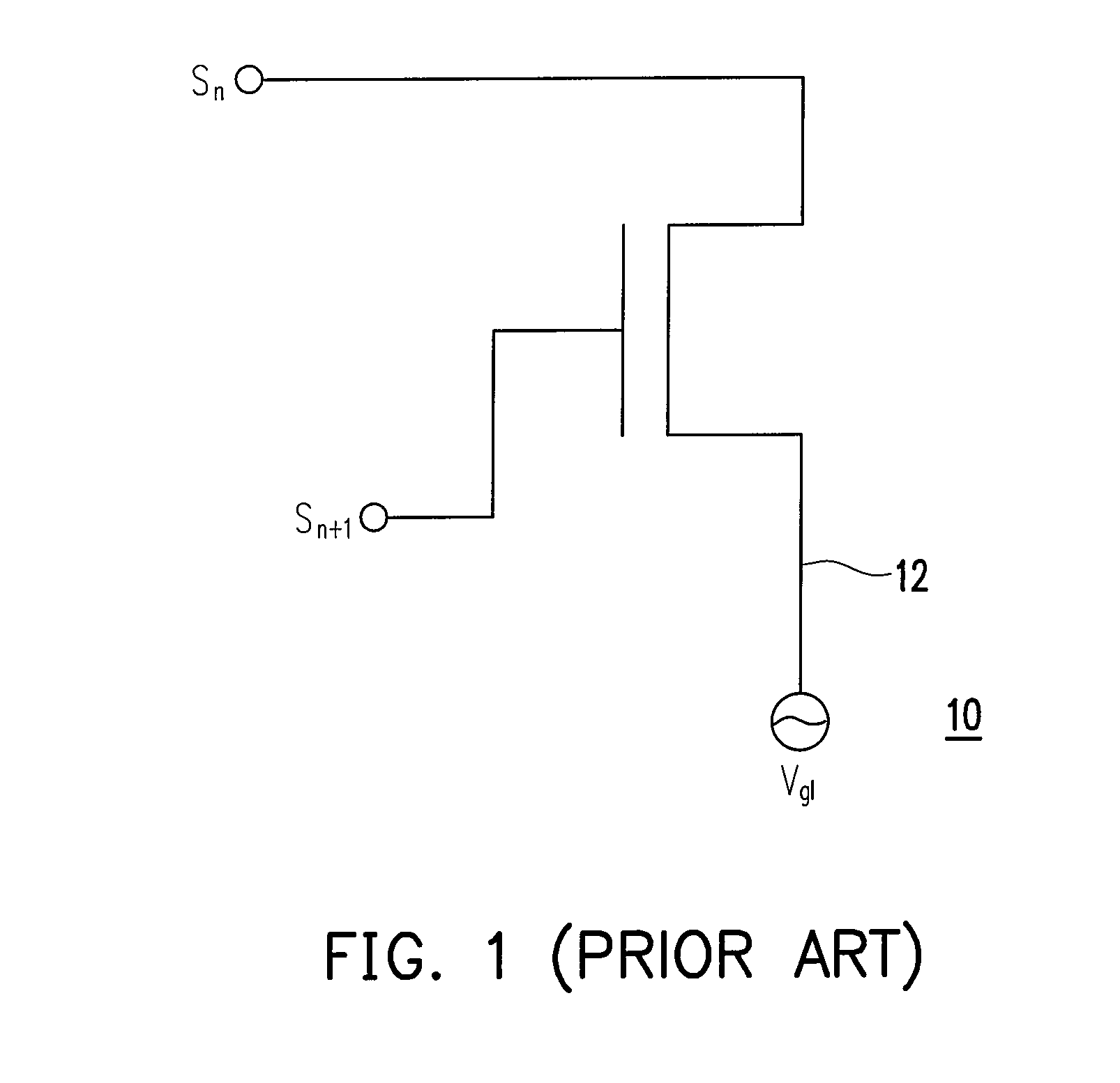
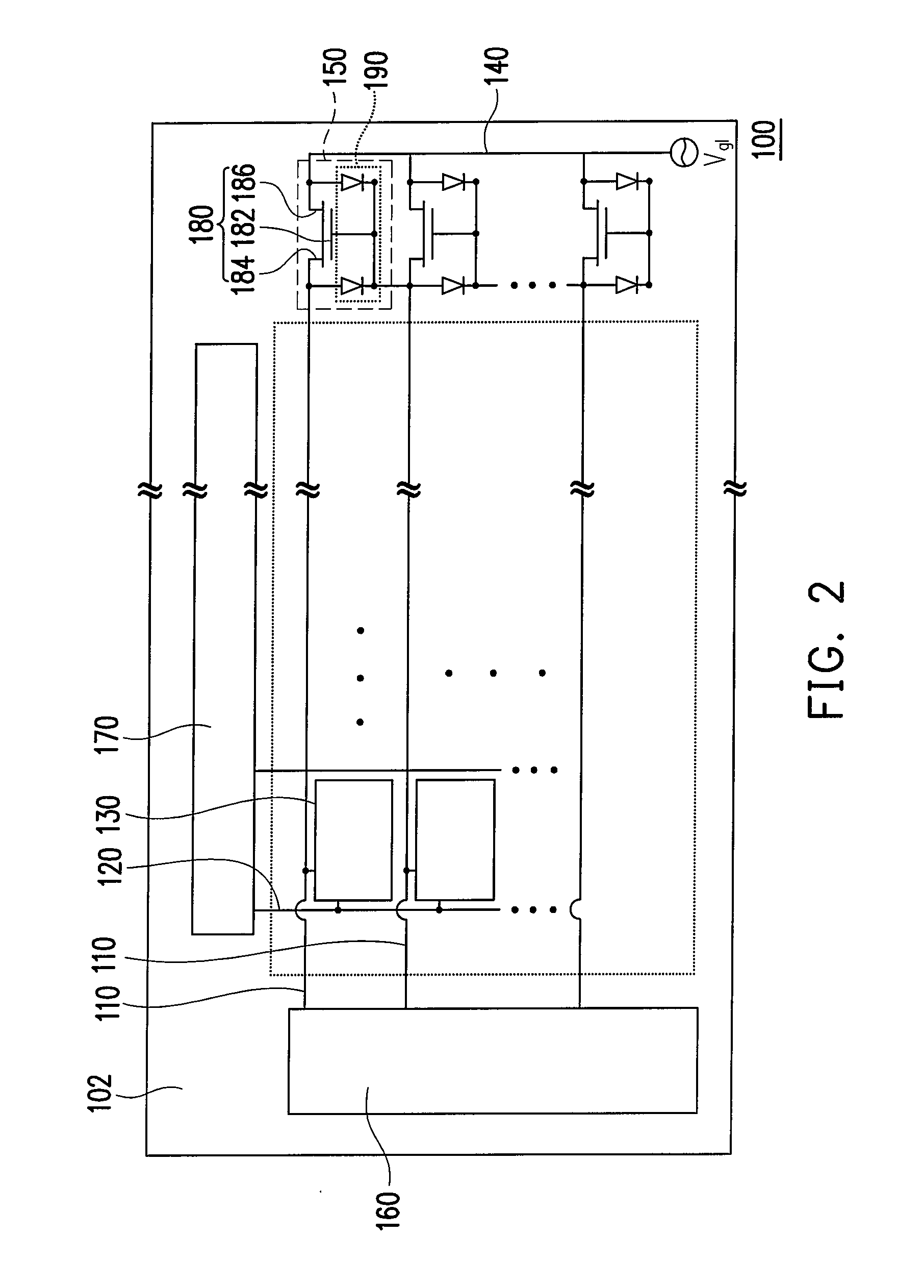
[0030]FIG. 2 is a schematic view of an active device array substrate according to an embodiment of the present invention. Referring to FIG. 2, an active device array substrate 100 includes a plurality of scan lines 110, a plurality of data lines 120, a plurality of pixels 130, a bus line 140 and a plurality of voltage pull-down circuits 150 all disposed on a substrate 102. The pixels 130 are arranged in array on the substrate 102, and are electrically connected to the scan lines 110 and the data lines 120 correspondingly. In the present embodiment, the active device array substrate 100 further includes a gate driving circuit 160 electrically connected to the scan lines 110 and a source driving circuit 170 electrically connected to the data lines 120. Each of the voltage pull-down circuits 150 including a transistor 180 and an electrostatic discharge protection device 190 is electrically connected between the scan line 110 and the bus line 140 correspondingly. In the present embodime...


PUM

PropertyMeasurementUnit
voltageaaaaaaaaaa
electricallyaaaaaaaaaa
sizeaaaaaaaaaa

Abstract

An active device array substrate including a substrate, scan lines, data lines, pixels, a bus line and voltage pull-down circuits is provided. The pixels disposed on intersections of the scan lines and the data lines are arranged in array on the substrate and are electrically connected to the scan lines and the data lines. Each of the voltage pull-down circuits including a transistor and an electrostatic discharge protection device is electrically connected between the scan line and the bus line correspondingly. Each transistor includes a source, a drain, and a gate electrically connected to a next scan line. Each gate is electrically connected to the scan line, the source, the drain and the bus line correspondingly through the electrostatic discharge protection device. The electrostatic discharge protection of the active device array substrate is enhanced effectively by the electrostatic discharge protection device.

Description

CROSS-REFERENCE TO RELATED APPLICATION[0001]This application claims the priority benefit of Taiwan application serial no. 96114547, filed Apr. 25, 2007. All disclosure of the Taiwan application is incorporated herein by reference.BACKGROUND OF THE INVENTION[0002]1. Field of the Invention[0003]The present invention relates to a liquid crystal display (LCD), and more particularly to an active device array substrate.[0004]2. Description of Related Art[0005]In recent years, since an optoelectronic technology and a semiconductor device manufacturing technology become more mature, flat panel displays have been accordingly developed. Among the flat panel displays, a liquid crystal display (LCD) is widely adopted to gradually replace a conventional CRT display and has become a main stream of displays on the market due to its advantages of low operation voltage, radiation free, light weight, small volume occupancy, and so forth.[0006]A thin film transistor liquid crystal display (TFT-LCD) is...

Claims


Application Information

Patent Timeline
Patent Type & Authority Applications(United States)
IPC IPC(8): G02F1/1333
CPCG02F1/136204G09G3/3648G09G2330/04
Inventor CHANG, LEE-HSUNTSAI, SHU-FENLIN, YU-WEN
Owner AU OPTRONICS CORP
Why Eureka
Try Eureka