Technique for enhancing dopant activation by using multiple sequential advanced laser/flash anneal processes

a laser/flash anneal process and laser activation technology, applied in semiconductor/solid-state device manufacturing, basic electric elements, electric apparatus, etc., can solve the problem that each individual step may have a moderately achieve low probability of creating respective device damage, enhance transistor performance, and increase the degree of dopant activation

Inactive Publication Date: 2008-10-30
ADVANCED MICRO DEVICES INC
View PDF13 Cites 10 Cited by
  • Summary
  • Abstract
  • Description
  • Claims
  • Application Information

AI Technical Summary

Benefits of technology

[0014]Generally, the subject matter disclosed herein is directed to a technique for enhancing the transistor performance by performing radiation-based anneal processes to obtain a desired high degree of dopant activation while not unduly contributing to diffusion of the dopant atoms. For this purpose, a plurality of short time radiation-based anneal processes may be performed, wherein each individual anneal step may be performed at appropriately selected energy and power settings so as to substantially not cause any damage in sensitive device areas, such as gate electrodes of transistor elements. It has been recognized that a series of radiation-based anneal processes may gradually increase the degree of dopant activation, while, on the other hand, each individual step may have a moderately low probability for creating respective device damage. Consequently, a desired reduction in series resistance in transistor devices may be obtained, while not contributing to enhanced device damage and undue dopant diffusion.

Problems solved by technology

It has been recognized that a series of radiation-based anneal processes may gradually increase the degree of dopant activation, while, on the other hand, each individual step may have a moderately low probability for creating respective device damage.

Method used


Image

  • Technique for enhancing dopant activation by using multiple sequential advanced laser/flash anneal processes
  • Technique for enhancing dopant activation by using multiple sequential advanced laser/flash anneal processes
  • Technique for enhancing dopant activation by using multiple sequential advanced laser/flash anneal processes

Examples


Embodiment Construction

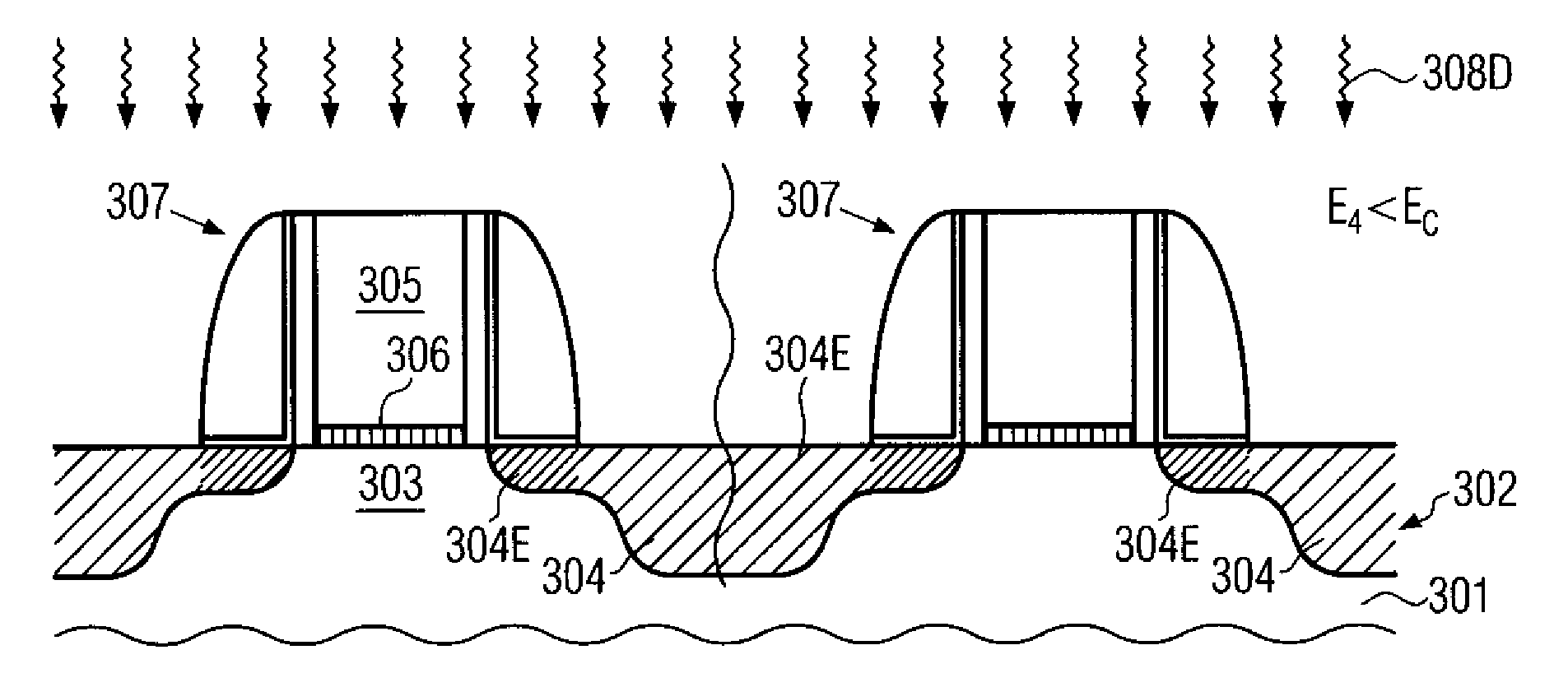
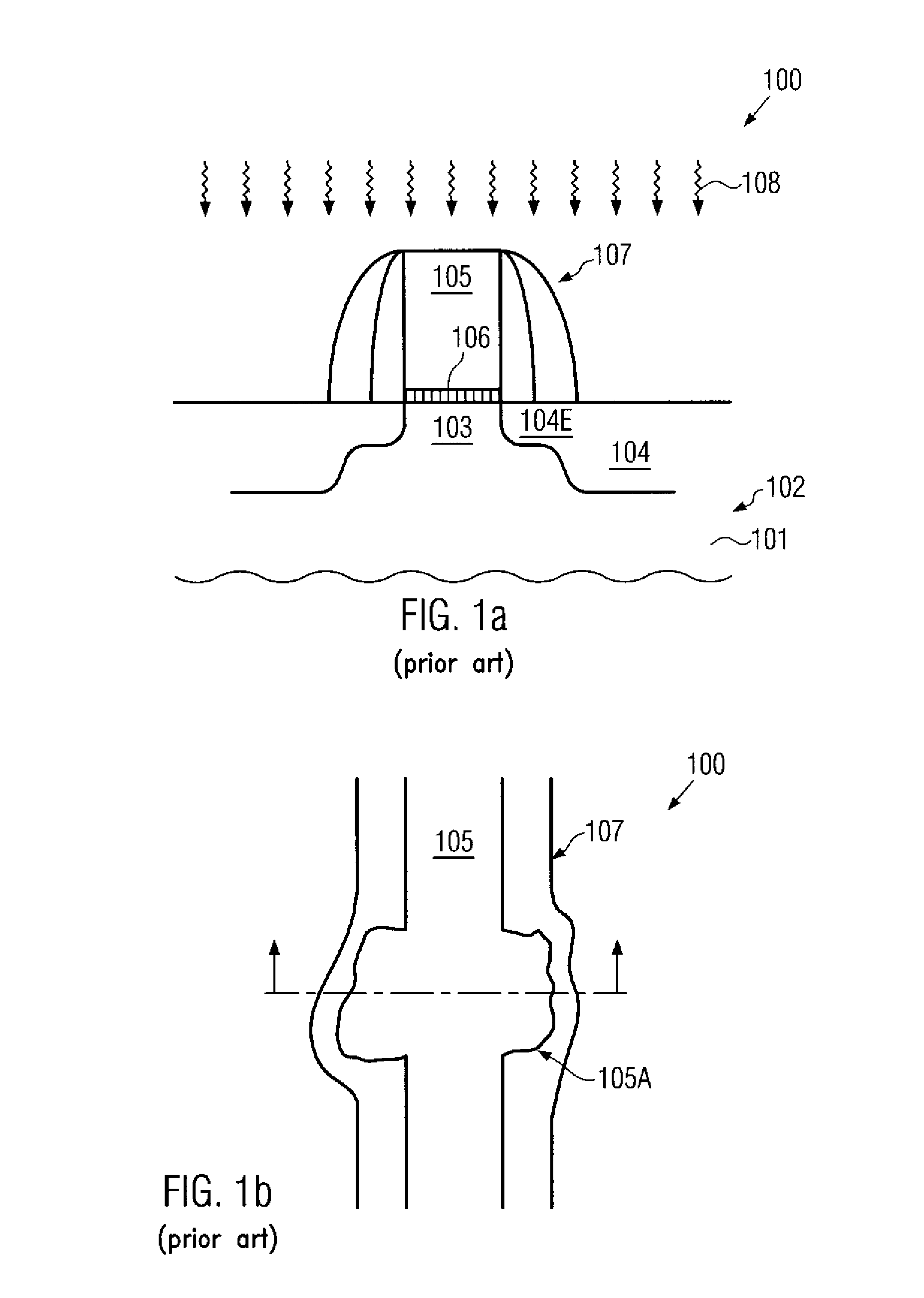
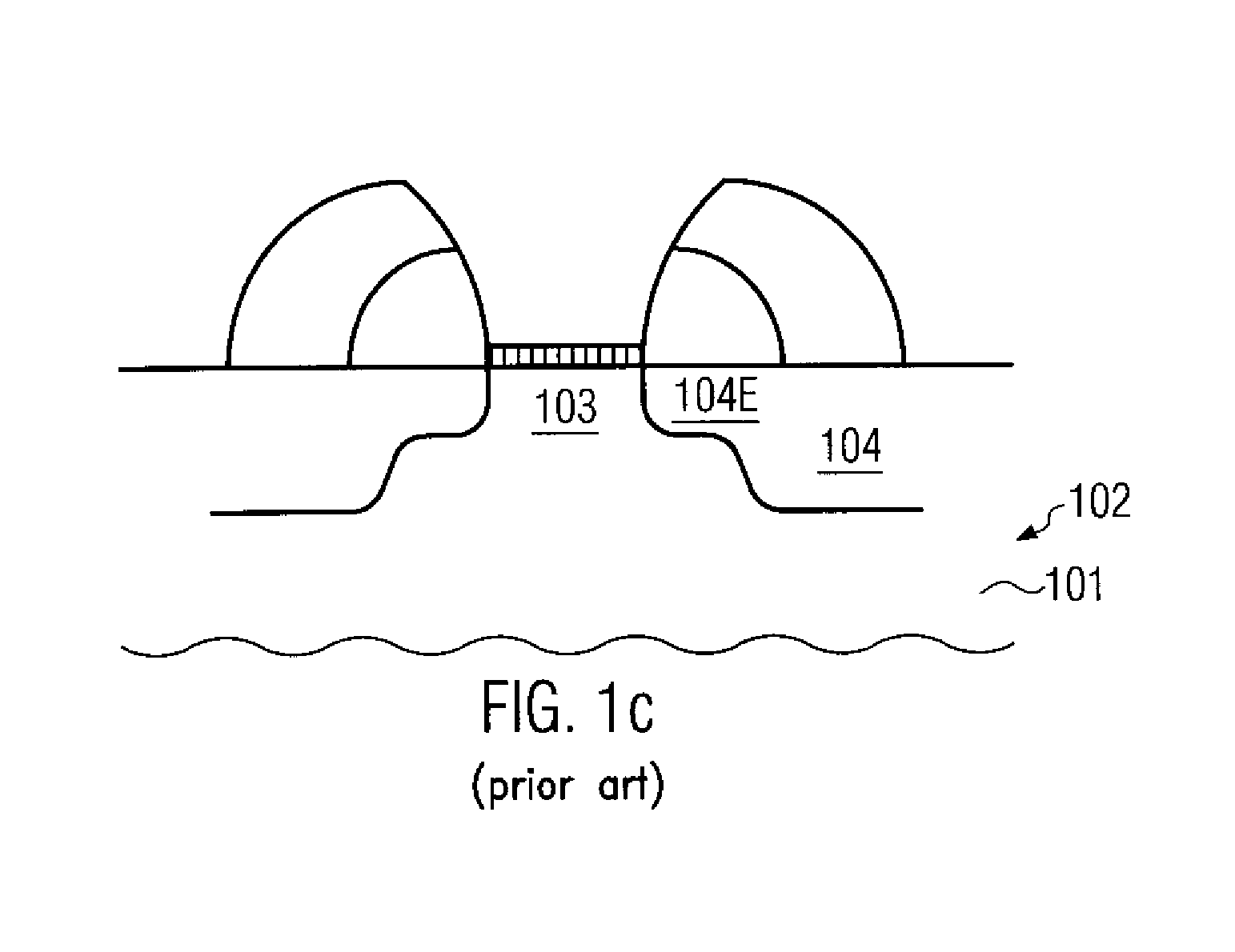
[0026]Various illustrative embodiments of the invention are described below. In the interest of clarity, not all features of an actual implementation are described in this specification. It will of course be appreciated that in the development of any such actual embodiment, numerous implementation-specific decisions must be made to achieve the developers' specific goals, such as compliance with system-related and business-related constraints, which will vary from one implementation to another. Moreover, it will be appreciated that such a development effort might be complex and time-consuming, but would nevertheless be a routine undertaking for those of ordinary skill in the art having the benefit of this disclosure.

[0027]The present subject matter will now be described with reference to the attached figures. Various structures, systems and devices are schematically depicted in the drawings for purposes of explanation only and so as to not obscure the present disclosure with details ...


PUM


Abstract

By performing multiple radiation-based anneal processes on the basis of less critical process parameters, the overall risk for creating anneal-induced damage, such as melting of gate portions, may be substantially avoided while nevertheless the respective degree of dopant activation may be enhanced for each individual anneal process. Consequently, the sheet resistance of advanced transistor devices may be reduced with a decreasing number of sequential anneal processes.

Description

BACKGROUND OF THE INVENTION[0001]1. Field of the Invention[0002]The present disclosure generally relates to the fabrication of integrated circuits, and, more particularly, to the fabrication of highly sophisticated field effect transistors, such as MOS transistor structures, requiring highly doped shallow junctions in combination with a low series resistance.[0003]2. Description of the Related Art[0004]The manufacturing process for integrated circuits continues to improve in several ways, driven by the ongoing efforts to scale down the feature sizes of the individual circuit elements. Presently, and in the foreseeable future, the majority of integrated circuits are and will be based on silicon devices due to the high availability of silicon substrates and due to the well-established process technology that has been developed over the past decades. A key issue in developing integrated circuits of increased packing density and enhanced performance is the scaling of transistor elements...

Claims


Application Information

Patent Timeline
Patent Type & Authority Applications(United States)
IPC IPC(8): H01L21/30H01L21/336
CPCH01L21/26513H01L21/268H01L21/823418H01L21/823814
Inventor WEI, ANDYFEUDEL, THOMASSCOTT, CASEY
Owner ADVANCED MICRO DEVICES INC
Why Eureka
Try Eureka