

Thin film transistor and method of manufacturing the same
- Summary
- Abstract
- Description
- Claims
- Application Information
AI Technical Summary
Benefits of technology
Problems solved by technology
Method used
Image

Examples
Embodiment Construction
[0028]The present invention will now be described more fully with reference to the accompanying drawings in which exemplary embodiments of the invention are shown. In the drawings, the thicknesses of layers and regions are exaggerated for clarity.
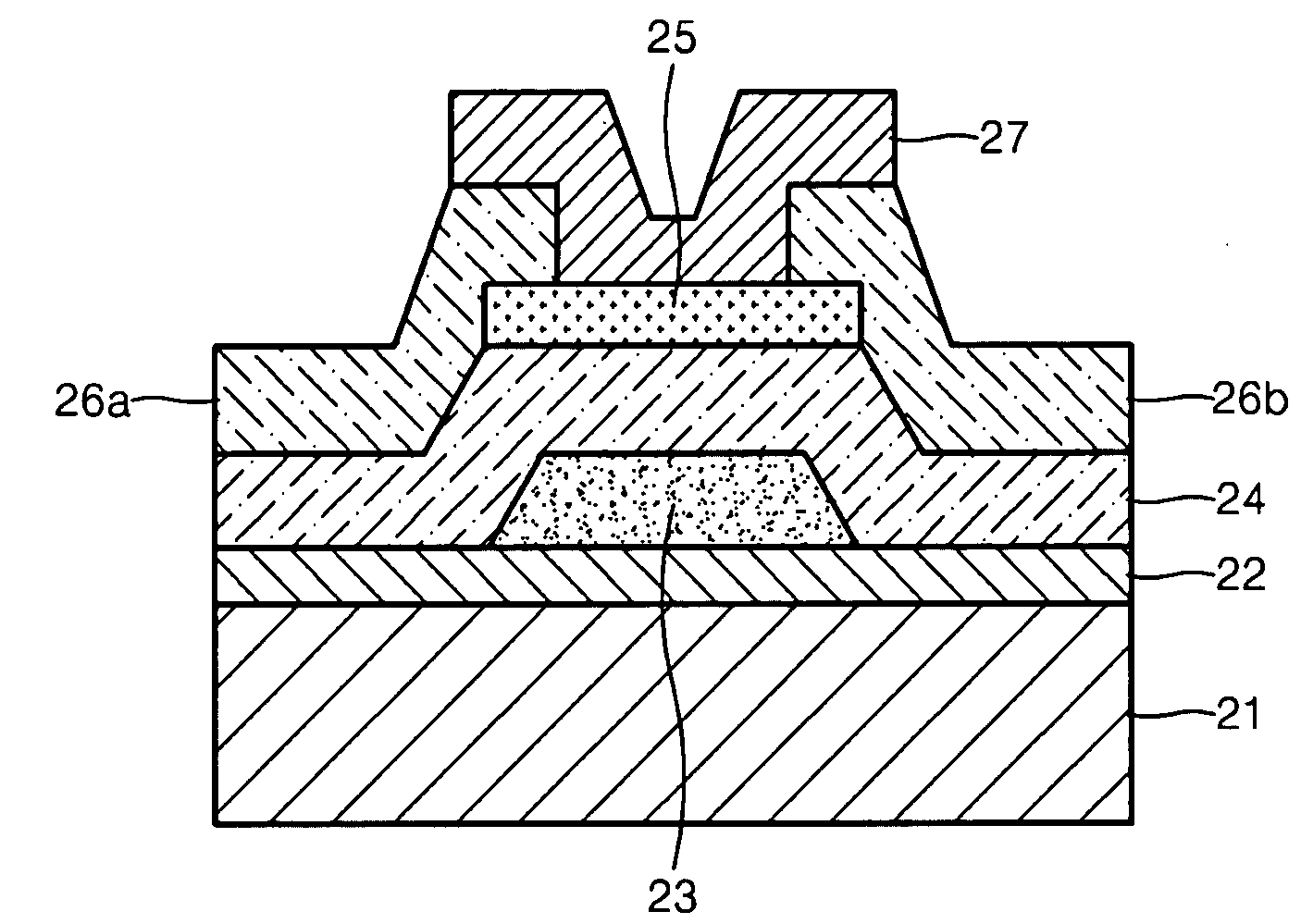
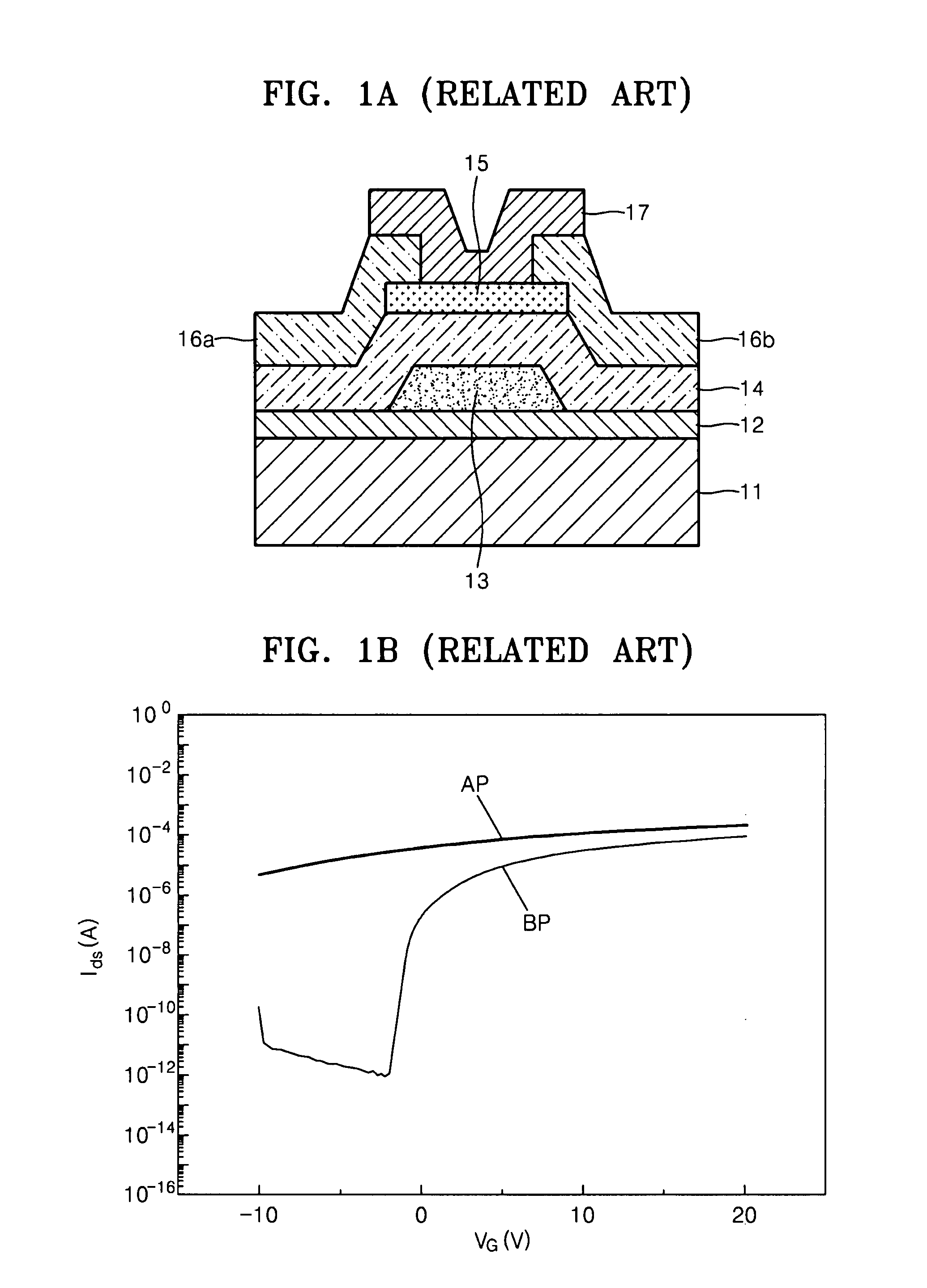
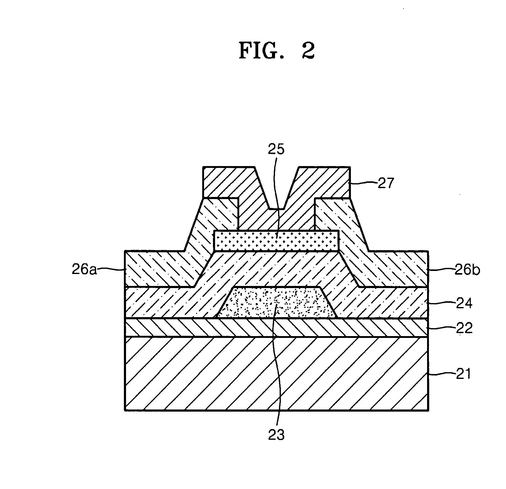
[0029]FIG. 2 is a cross-sectional view of a thin film transistor according to an embodiment of the present invention. The thin film transistor of FIG. 2 is a bottom gate type thin film transistor.
[0030]Referring to FIG. 2, an insulating layer 22 is formed on a substrate 21, and a gate 23 is formed on a region of the insulating layer 22. A gate insulating layer 24 is formed on the insulating layer 22 and the gate 23, and a channel region 25 is formed on a region of the gate insulating layer 24 corresponding to the location of the gate 23. A source 26a and a drain 26b are formed on either side of a portion of the channel region 25. A passivation layer 27 is formed on the channel region 25.
[0031]Materials for forming the layers of the thin fil...
PUM
 Abstract
Description
Claims
Application Information