

Reflection-type banpass filter
- Summary
- Abstract
- Description
- Claims
- Application Information
AI Technical Summary
Benefits of technology
Problems solved by technology
Method used
Image

Examples
embodiment 1
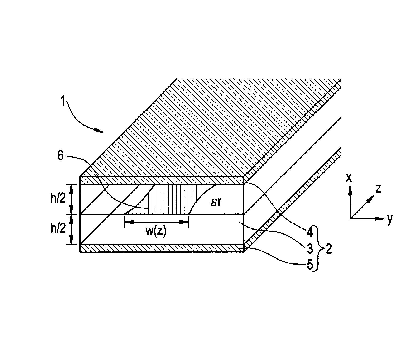
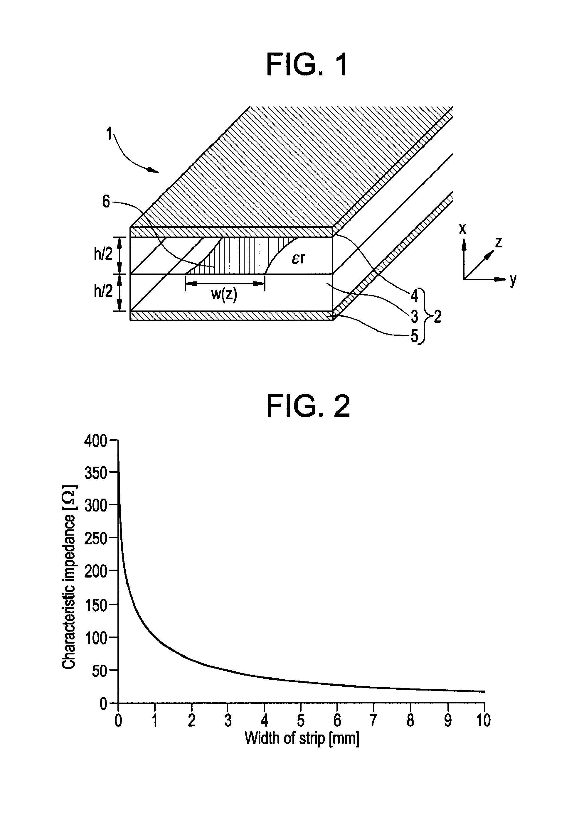
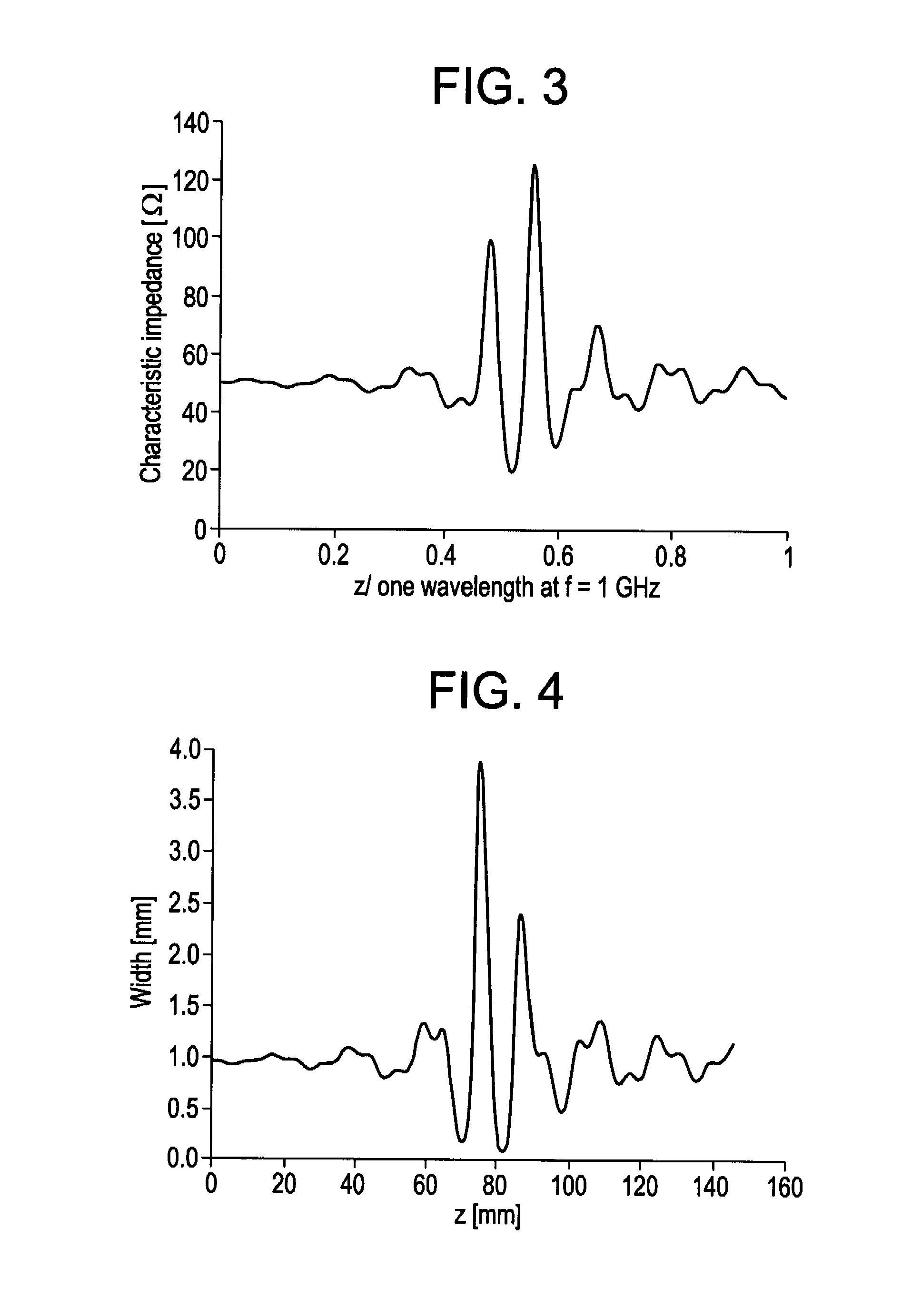
[0089] A Kaiser window was used for which the reflectance is 1 at frequencies f in the range 3.4 GHz≦f≦10.3 GHz, and is 0 elsewhere, and for which A=30. Design was performed using one wavelength of signals at frequency f=1 GHz propagating in the microstrip as the waveguide length, and setting the system characteristic impedance to 50Ω. FIG. 3 shows the distribution in the z-axis direction of the local characteristic impedance obtained in the inverse problem. The horizontal axis is z divided by one wavelength at f=1 GHz; similar axes are used in FIG. 8, FIG. 13, FIG. 18, and FIG. 23 below. “z” is the length extending in the z-axis direction from the end face on the input end. The horizontal axis indicates the value which is obtained by dividing z by one wavelength at f=1 GHz.
[0090]FIG. 4 shows the distribution in the z-axis of the center conductor width w, when using a dielectric layer 3 of thickness h=2 mm and with relative permittivity ∈r=4.2. Tables 1 through 3 list the center co...
embodiment 2
[0095] A Kaiser window was used for which the reflectance is 1 at frequencies f in the range 3.4 GHz≦f≦10.3 GHz, and is 0 elsewhere, and for which A=30. Design was performed using one-half the wavelength of signals at frequency f=1 GHz propagating in the microstrip as the waveguide length, and setting the system characteristic impedance to 50Ω. FIG. 8 shows the distribution in the z-axis direction of the local characteristic impedance obtained in the inverse problem.
[0096]FIG. 9 shows the z-axis distribution of the center conductor width w, when using a dielectric layer 3 of thickness h=3 mm and with relative permittivity ∈r=2. Tables 4 through 6 list the center conductor widths w.
TABLE 4Center conductor widths (1 / 3)z[mm]0.000.110.210.320.420.830.640.740.850.951.061.17w[mm]2.682.682.682.682.692.692.692.702.702.702.712.71 #21.271.581.481.501.701.801.912.022.122.232.332.44—2.712.712.712.722.722.722.722.722.722.722.722.73 #32.552.652.702.802.973.083.183.293.393.503.613.71—2.732.732....
embodiment 3
[0101] A Kaiser window was used for which the reflectance is 0.9 at frequencies f in the range 4.0 GHz≦f≦9.6 GHz, and is 0 elsewhere, and for which A=30. Design was performed using the wavelength of signals at frequency f=0.3 GHz propagating in the microstrip as the waveguide length, and setting the system characteristic impedance to 50Ω. FIG. 13 shows the distribution in the z-axis direction of the local characteristic impedance obtained in the inverse problem.
[0102]FIG. 14 shows the z-axis distribution of the center conductor width w, when using a dielectric layer 3 of thickness h=2 mm and with relative permittivity ∈r=4.2. Tables 7 and 8 list the center conductor widths.
TABLE 7Center conductor widths (1 / 2)s[mm]0.000.070.150.220.290.370.440.510.590.660.730.81w[mm]0.960.960.960.960.960.950.950.950.950.940.940.94 #20.880.951.021.101.171.241.321.391.461.541.611.68—0.930.930.930.930.920.920.920.920.910.910.910.90 #31.761.831.901.982.052.122.202.272.342.422.492.56—0.900.900.900.900....
PUM
 Abstract
Description
Claims
Application Information