

Metal microscopic structure and detection device
- Summary
- Abstract
- Description
- Claims
- Application Information
AI Technical Summary
Benefits of technology
Problems solved by technology
Method used
Image

Examples
embodiments
Outline of Detection System
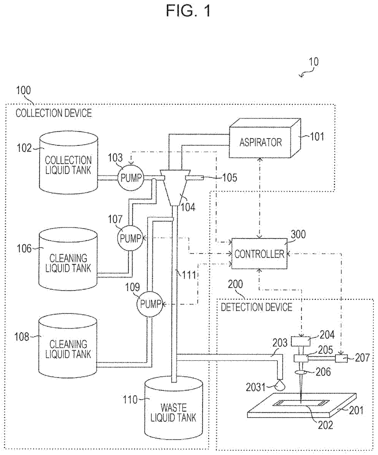
[0046]A metal microscopic structure and a detection device according to an embodiment may be each, for example, a component of a detection system described below. FIG. 1 is a block diagram illustrating an example of a detection system 10 according to the embodiment. The detection system 10 is installed in a room for people to enter and exit. The detection system 10 collects, for example, fine particles possibly containing an analyte, such as a virus floating in the air, and detects the concentration of the analyte contained in the fine particles. This embodiment is described in connection with the case in which the analyte is a virus or a virus component (hereinafter simply called a “virus”). The virus component is, for example, a protein or a nucleic acid forming the virus. The type of virus is not limited to particular one, and may be what is generally classified as a virus. The analyte needs not to be the virus, and may be, for example, a bacterium or a...
example 1
[0131]A gold film was formed in a thickness of 300 nm on the above-mentioned resin substrate by the electron beam vapor deposition, and another gold film was then formed in a thickness of 100 nm by the sputtering. FIG. 7A represents a sectional SEM image of the metal microscopic structure obtained in this Example.
example 2
[0132]A gold film was formed in a thickness of 300 nm on the above-mentioned resin substrate by the electron beam vapor deposition, and another gold film was then formed in a thickness of 300 nm by the sputtering. A sectional SEM image of the metal microscopic structure obtained in this Example was similar to that represented in FIG. 7A. Hence the sectional SEM image in this Example is omitted.
[0133]The sensor substrate included the metal microscopic structure described above. A SAM was formed on the metal microscopic structure by dipping the sensor substrate into a SAM solution in an incubator at 40° C.
[0134]The SAM solution was prepared through the following procedures. First, Carboxy-EG6-undecanethiol and Hydroxy-EG3-undecanethiol were mixed after diluting each of them into a solution of 1 mM (10−3 mol / L) with ethanol. Then, the SAM solution was obtained by diluting the mixture 5 times with ethanol.
[0135]Thereafter, a terminal carboxyl group of the SAM and a terminal amino group ...
PUM
 Abstract
Description
Claims
Application Information