A tsv Interposer structure and its encapsulation method

A packaging method and one-sided technology, applied in the direction of electrical components, electrical solid devices, circuits, etc., can solve problems such as cracked silicon holes or insulating layers, low yield, and difficult process control, so as to achieve sufficient insulating layer thickness and improve yield , The effect of reducing the difficulty of the process

Active Publication Date: 2017-06-23
JIANGYIN CHANGDIAN ADVANCED PACKAGING CO LTD
View PDF4 Cites 0 Cited by
  • Summary
  • Abstract
  • Description
  • Claims
  • Application Information

AI Technical Summary

Problems solved by technology

The TSV production of Silicon Interposer is traditionally complicated, and the diameter of the silicon hole is limited, usually within 30 microns; if the silicon hole is made larger, the metal filled in the silicon hole will be heated and expanded during later use, resulting in the silicon hole or insulation crack
Therefore, the silicon hole can only be made smaller; but the insulation deposition, barrier / seed layer deposition, and filling metal in the small silicon hole will become difficult
Therefore, the process control is more difficult, and the yield rate is relatively low

Method used


Image

  • A tsv Interposer structure and its encapsulation method
  • A tsv Interposer structure and its encapsulation method
  • A tsv Interposer structure and its encapsulation method

Examples


Embodiment Construction

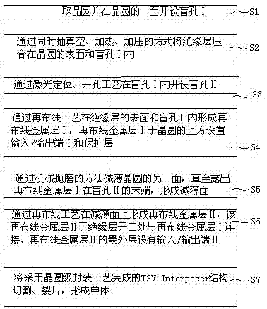
[0056] see figure 1 , the technological process of the encapsulation method of a kind of TSV Interposer structure of the present invention is as follows:

[0057] S1: Take the wafer and open a blind hole I on one side of the wafer;

[0058] S2: Pressing the insulating layer on the surface of the wafer and inside the blind hole I by vacuuming, heating, and pressing at the same time;

[0059] S3: Open blind hole II in blind hole I through laser positioning and hole opening process;

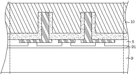
[0060] S4: Form the rewiring metal layer I on the surface of the insulating layer and the blind hole II through the rewiring process, and set the input / output terminal I and the protective layer above the wafer on the rewiring metal layer I;

[0061] S5: The other side of the wafer is thinned by mechanical polishing until the rewiring metal layer I is exposed at the end of the blind hole II to form a thinned surface;

[0062] S6: Form the rewiring metal layer II on the thinned surface through the...


PUM


Abstract

The invention discloses a TSV Interposer structure and a packaging method of the TSV Interposer structure and belongs to the field of semiconductor packaging technologies. The packaging method includes the steps that a wafer is taken and a blind hole I is formed in one face of the wafer; an insulation layer is in press fit on the surface of the wafer and in the blind hole I in the manner of carrying out vacuumizing, heating and pressurizing simultaneously; a blind hole II is formed in the blind hole I through positioning and laser hole forming technologies; a rewiring metal layer I is arranged on the surface of the insulation layer and in the blind hole II through a rewiring technology, and an input / output end I and a protection layer are arranged on the portion, above the wafer, of the rewiring metal layer I; the other face of the wafer is thinned through a mechanical polish-grinding method to from a thinned face; a rewiring metal layer II is formed on the thinned face through the rewiring technology, and the rewiring metal layer II is connected with the rewiring metal layer I at an opening of the insulation layer; the TSV Interposer structure completed through a wafer level packaging technology is cut and crushed. According to the TSV Interposer structure and the packaging method of the TSV Interposer structure, the process difficulty is effectively reduced, and the yield of an Interposer is improved.

Description

technical field [0001] The invention relates to a TSV Interposer structure and a packaging method thereof, belonging to the technical field of semiconductor packaging. Background technique [0002] The Silicon Interposer in Interposer is a device similar to a circuit board made of silicon wafers, but its line width and node spacing are smaller than that of a circuit board. Chips with different functions, such as CPU and DRAM, can be connected to the same silicon interposer, and many calculations and data exchanges can be completed through the Silicon Interposer, which saves power and increases bandwidth. Similar to PCBs, Silicon Interposers generally have copper-filled through holes (TSVs), and the results of joint operations between different chips are transmitted to the connected circuit boards through TSVs. So Silicon Interposer is equivalent to a bridge between multiple chips and the same circuit board. The TSV production of Silicon Interposer is traditionally complex,...

Claims


Application Information

Patent Timeline
Patent Type & Authority Patents(China)
IPC IPC(8): H01L23/48H01L23/495H01L21/56
CPCH01L2224/16
Inventor 胡正勋符召阳梅万元章力陈西平陈栋张黎陈锦辉赖志明
Owner JIANGYIN CHANGDIAN ADVANCED PACKAGING CO LTD
Why Eureka
Try Eureka