Semiconductor device fabrication method

Inactive Publication Date: 2007-11-29
LAPIS SEMICON CO LTD
View PDF3 Cites 0 Cited by
  • Summary
  • Abstract
  • Description
  • Claims
  • Application Information

AI Technical Summary

Benefits of technology

[0020] The present invention has been devised in consideration of the problem described above, and an object of this invention is to provide a method for fabricating a silicon device which method prevents conduction failures of a contact plug that is provided penetrating through a silicon oxide layer, a silicon nitride layer and an inter-layer insulation layer, and prevents leaching of a wiring metal into a silicon substrate.
[0023] According to the semiconductor device fabrication method of the first aspect, the thickness of the silicon oxide layer, being a value somewhere in the range from 32 to 48 nm, is thin in comparison with a conventional 90 nm. Therefore, a portion of a titanium conduction film that is not formed with sufficient thickness at a lower portion of the contact hole is reduced and, as a result, excellent titanium silicide can be formed.
[0024] Furthermore, according to the semiconductor device fabrication method of the second aspect, because the aperture portion is formed in the silicon nitride layer and thereafter the inter-layer insulation layer is formed and the contact hole is formed within the aperture portion, the silicon nitride layer will not remain in a flange form at the inner wall of the contact hole. Therefore, a titanium conduction film is formed with sufficient thickness even at a lower portion of the contact hole and, as a result, excellent titanium silicide can be formed.

Problems solved by technology

In such a case, if the semiconductor device is left in the atmosphere for about 20 hours from after the contact hole is formed until when formation of the titanium conduction film 180, the titanium silicide 182 and the contact plug 185 is implemented, there is a problem in that anomalous leak currents occur in the semiconductor device and it cannot be used as a product.
As a result, the formation of the titanium silicide at the lower portion of the contact hole is impeded, which leads to failures in conduction with a contact.
In addition, p-n junction breakdown occurs in the diffusion layer, due to leaching of a wiring metal into the silicon substrate or the like, and as a result, leakage currents occur.

Method used


Image

  • Semiconductor device fabrication method
  • Semiconductor device fabrication method
  • Semiconductor device fabrication method

Examples


first embodiment

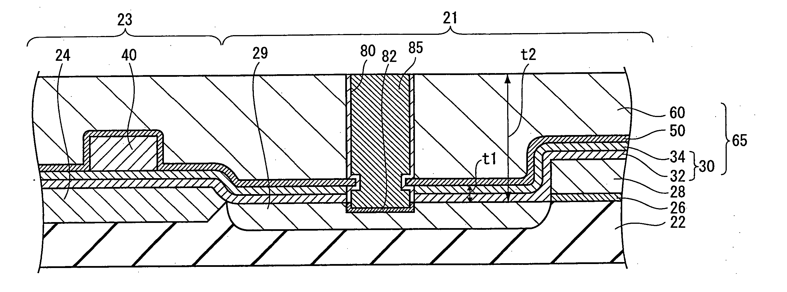
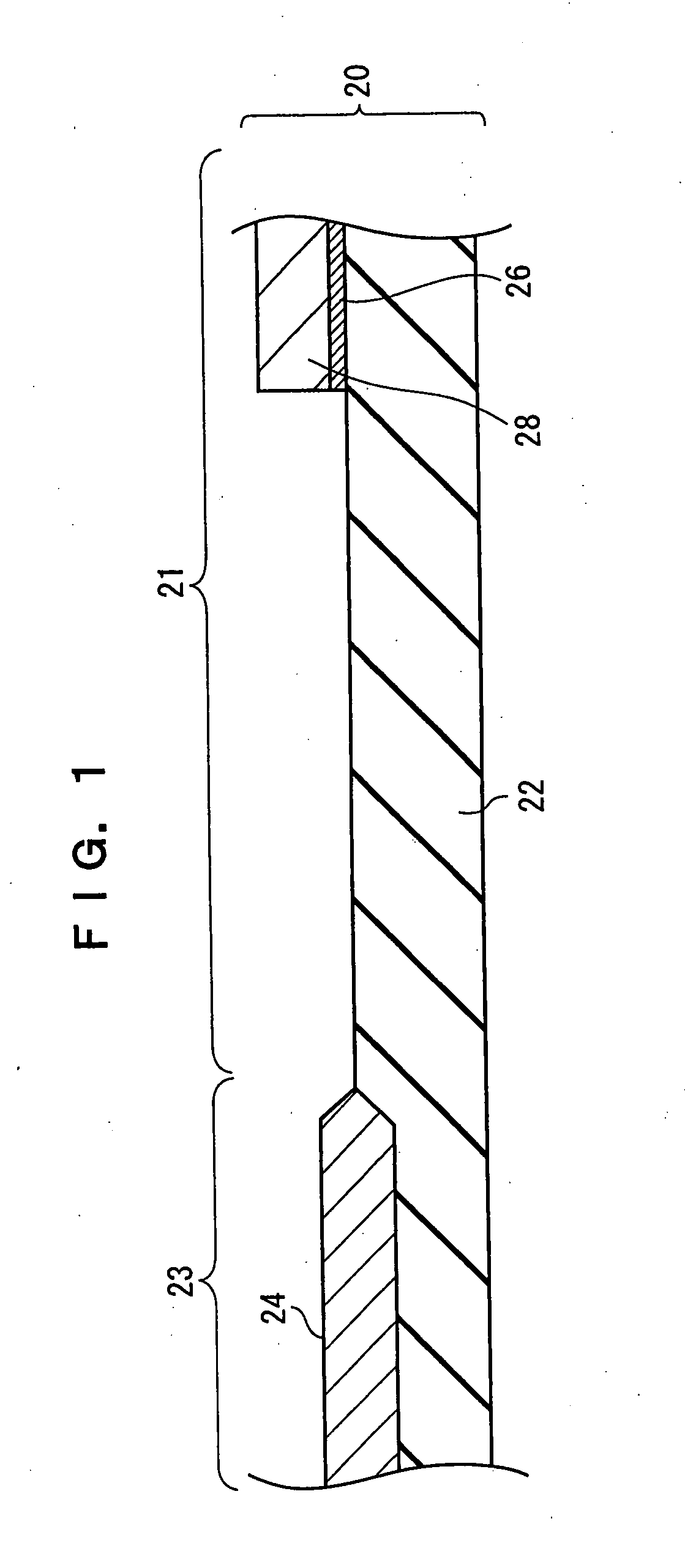
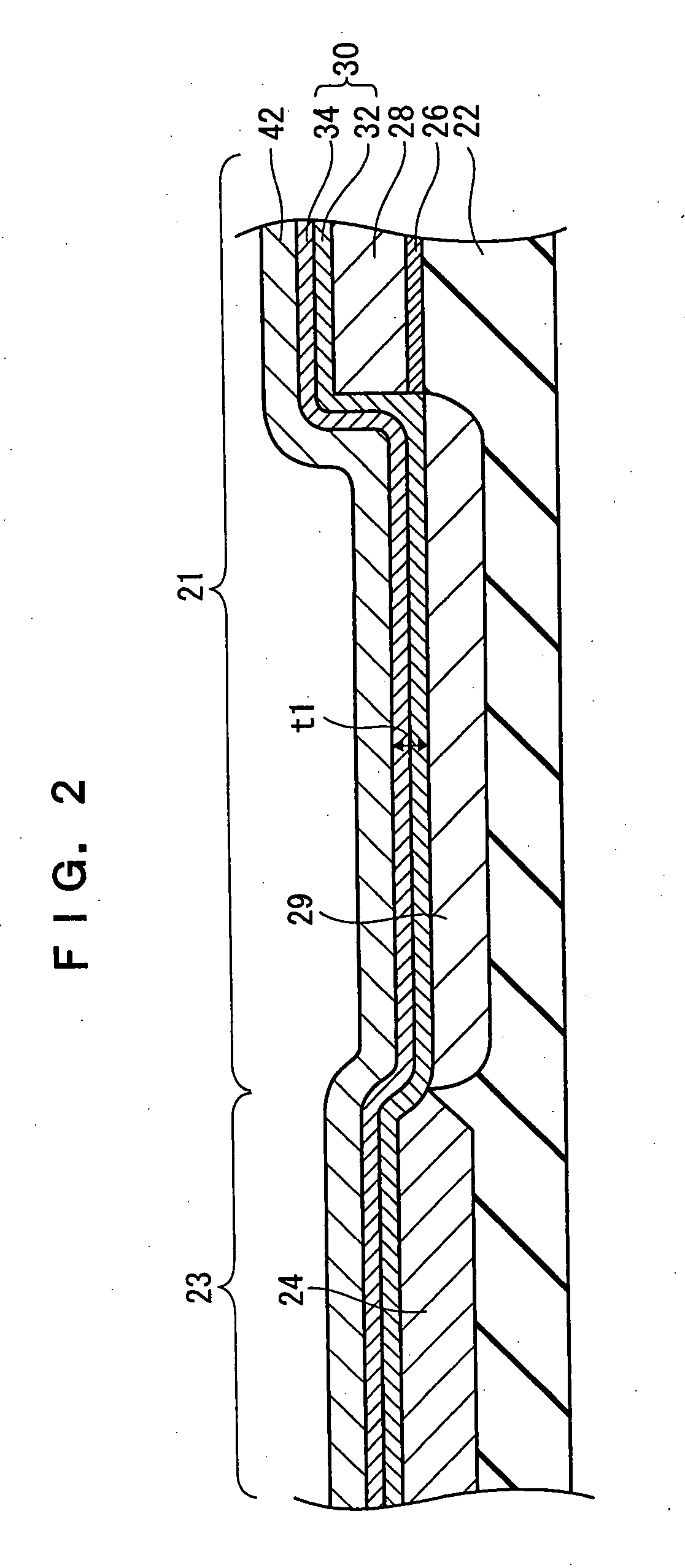
[0038] A semiconductor device fabrication method of a first embodiment will be described with reference to FIGS. 1 to 7. FIGS. 1 to 7 are process diagrams for explaining the semiconductor device fabrication method of the first embodiment, and are shown cut along a sectional plane.

[0039] Firstly, an underlying structure 20 is prepared. The underlying structure 20 is provided with a silicon substrate 22, an element isolation layer 24 formed on the silicon substrate 22, and a gate oxide film 26 and a gate electrode 28 which are layered in that order on one major surface of the silicon substrate 22.

[0040] An element isolation region 23 and a MOS transistor formation region 21 are provided at the underlying structure 20. The element isolation region 23 is a region at which the element isolation layer 24 is formed, and the MOS transistor formation region 21 is a region defined by the element isolation region 23. The gate oxide film 26 and the gate electrode 28 are formed on the underlyi...

second embodiment

[0056] A semiconductor device fabrication method of a second embodiment will be described with reference to FIGS. 8 and 9. FIGS. 8 and 9 are process diagrams for explaining the semiconductor device fabrication method of the second embodiment, and are shown cut along a sectional plane.

[0057] Steps up to the formation of the silicon nitride layer are similar to those described with reference to FIGS. 1 and 2 and FIGS. 3 and 4, and will not be described here. In the second embodiment however, the thickness of the resistance isolation oxide layer 34 is not limited to 20±5 nm, and may be around 70 nm, similarly to a conventional case. When the thickness of the resistance isolation oxide layer 34 is greater, the effect of preventing the phosphorus and boron included in the BPSG layer from reaching the transistor is enhanced.

[0058] After a silicon nitride layer 51 has been formed, an aperture portion 55, which exposes the silicon oxide layer 30, is formed in the silicon nitride layer 51....


PUM


Abstract

In fabrication of a semiconductor device which is provided with resistances and MOS transistors on the same substrate, preventing conduction failures of contacts and preventing leaching of wiring metal into a silicon substrate. Firstly, an underlying structure is prepared. Then, a silicon oxide layer is formed on the underlying structure. Then, a silicon nitride layer is formed on the silicon oxide layer. Then, an inter-layer insulation layer is formed on the silicon nitride layer. Then, a contact hole is formed penetrating through a laminate of the silicon oxide layer, the silicon nitride layer and the inter-layer insulation layer. A thickness of the silicon oxide layer is a value in a range from 32 to 48 nm.

Description

CROSS-REFERENCE TO RELATED APPLICATION [0001] This application claims priority under 35 USC 119 from Japanese Patent Application No. 2006-098100, the disclosure of which is incorporated by reference herein. BACKGROUND OF THE INVENTION [0002] 1. Field of the Invention [0003] The present invention relates to a method for fabricating a semiconductor device. [0004] 2. Description of the Related Art [0005] Among semiconductor devices which are currently mass-produced, there are semiconductor devices which, in order to improve functionality, are provided with a mixture of resistors and MOS transistors on the same substrate (see, for example, Japanese Patent Application Laid-Open (JP-A) No. 2004-119697). A resistor thereof is provided by, for example, implanting an impurity into a polysilicon layer formed on the substrate and then etching the polysilicon layer. [0006] A conventional semiconductor device in which resistances and MOS transistors are formed on the same substrate will be descr...

Claims


Application Information

Patent Timeline
IPC IPC(8): H01L21/8234
CPCH01L21/76802H01L21/76832H01L23/485H01L27/0629H01L2924/0002H01L28/20H01L2924/00
Inventor YONEKURA, HIROSHI
Owner LAPIS SEMICON CO LTD
Why Eureka
Try Eureka