Signal sensing circuit and semiconductor memory device using the same

Active Publication Date: 2008-11-13
ETRON TECH INC
View PDF6 Cites 2 Cited by
  • Summary
  • Abstract
  • Description
  • Claims
  • Application Information

AI Technical Summary

Benefits of technology

[0007]It is the primary object of the present invention to provide a signal sensing circuit that keeps all

Problems solved by technology

That is a problem for the performance improving of the memory system.
After that, the voltage kick is no more helpful for the small signal sensing.
Furthermore, it would become diff

Method used


Image

  • Signal sensing circuit and semiconductor memory device using the same
  • Signal sensing circuit and semiconductor memory device using the same
  • Signal sensing circuit and semiconductor memory device using the same

Examples


Embodiment Construction

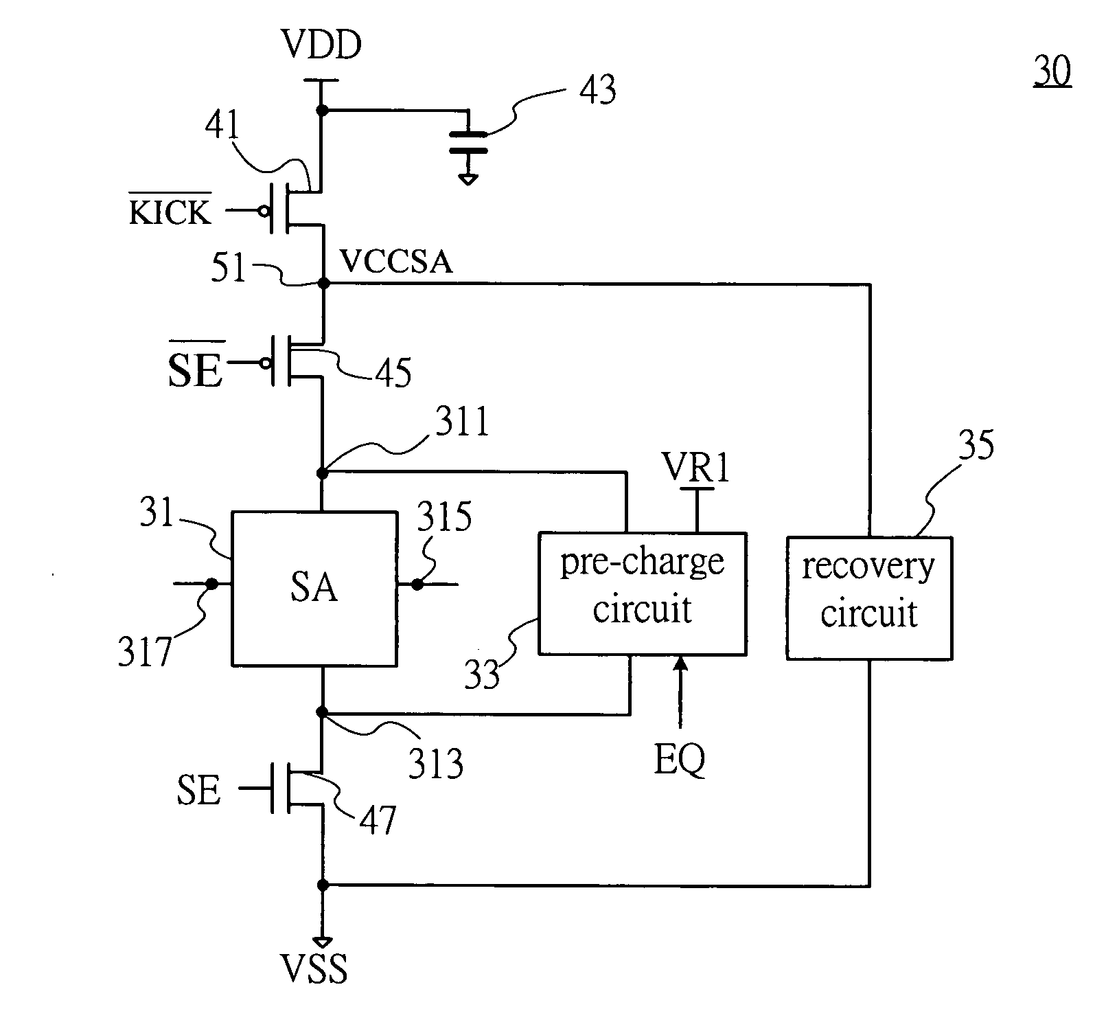
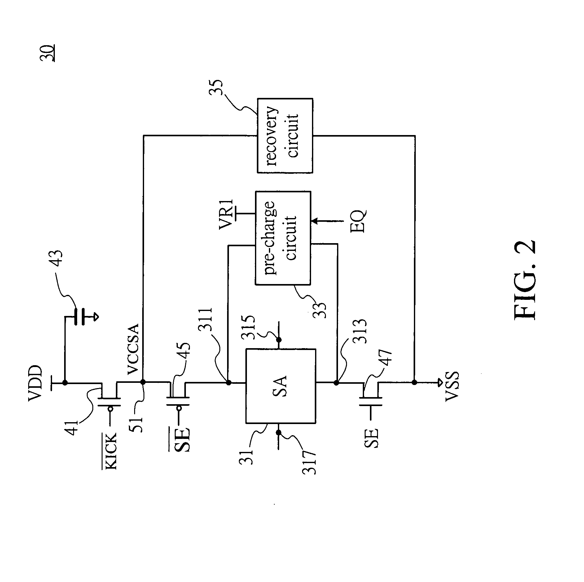
[0024]Referring to FIG. 2, FIG. 3, and FIG. 4, there are shown a block diagram of the sensing circuit, the circuit diagrams of the sense amplifier and the recovery circuit respectively of a preferred embodiment of the present invention. As shown in FIG. 2, the signal sensing circuit 30 comprises a sense amplifier 31, a kick transistor 41, a first control transistor 45, a second control transistor 47, a pre-charge circuit 33 and a recovery circuit 35.

[0025]The sense amplifier 31 comprises a first transistor 321, a second transistor 323, a third transistor 325 and a fourth transistor 327, as shown in FIG. 3. The first transistor 321 is a PMOS with the source connected to the source of the third transistor 325 at a node defined as the first power terminal 311, the drain connected to the drain of the second transistor 323 at a node defined as the second sense terminal 317. The second transistor 323 is a NMOS with the source connected to the source of the fourth transistor 327 at a node ...


PUM


Abstract

A signal sensing circuit and a semiconductor memory device using the same are provided. The signal sensing circuit comprises a sense amplifier, a kick transistor, a first control transistor, a second control transistor, a pre-charge circuit, and a recovery circuit. The kick transistor is used to pull up the operation voltage of the sense amplifier to improve the small signal sensing speed of the sense amplifier. After the signal is sensed, the recovery circuit will pull down the operation voltage of the sense amplifier to the standard level. In the present invention, the small signal sensing speed is greatly improved and the operation voltage of sense amplifier is kept away from the saturated level.

Description

FIELD OF THE INVENTION[0001]The present invention relates to a signal sensing circuit and a semiconductor memory device using the same, and more particularly to a signal sensing circuit with a recovery circuit and a semiconductor memory device using the same.BACKGROUND OF THE INVENTION[0002]In order to improve the data transfer rate of a memory system, such as a dynamic random access memory (DRAM) system, people raise the clock frequency of the system. For the same purpose, the operation voltage for the memory device is reduced, too. During the read cycle of the memory system, it takes more time for the sense amplifier to catch the small signal form the array of memory cells in low operation voltage. That is a problem for the performance improving of the memory system.[0003]Referring to FIG. 1, there is shown a timing diagram of the operation voltage of the sense amplifier of the semiconductor memory device of the prior art. In order to overcome the drawbacks of the prior art, peopl...

Claims


Application Information

Patent Timeline
IPC IPC(8): G11C7/04G01R19/00
CPCG11C7/08G11C7/12G11C11/4091
Inventor SHIAH, CHUNWU, CHUN-PENGCHANG, CHENG-NAN
Owner ETRON TECH INC
Why Eureka
Try Eureka