Methods of manufacturing mos transistors with strained channel regions

Inactive Publication Date: 2008-11-13
SAMSUNG ELECTRONICS CO LTD
View PDF10 Cites 23 Cited by
  • Summary
  • Abstract
  • Description
  • Claims
  • Application Information

AI Technical Summary

Benefits of technology

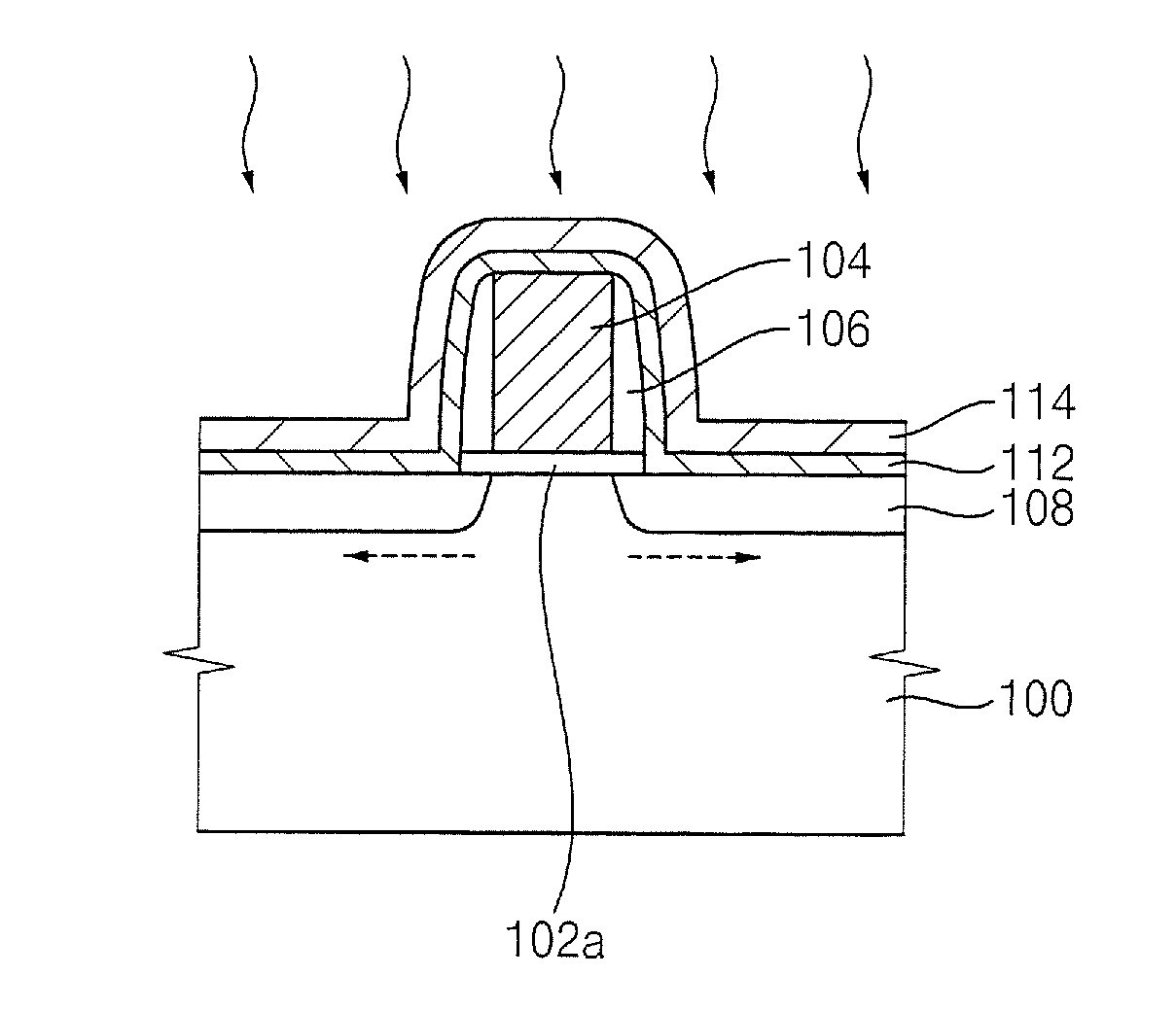
[0030]Some embodiments of the present invention may thereby manufacture a PMOS transistor having improved electrical characteristics by the formation of a strained region in a substrate portion thereof. Further, an N type MOS (NMOS) transistor and the PMOS transistor ma

Problems solved by technology

Since the stresses in the channel regions of the NMOS and the PMOS transistors having high performances are different from each other, it can be difficult to form such NMOS and the PMOS transistors on a common substrate.
When the c

Method used


Image

  • Methods of manufacturing mos transistors with strained channel regions
  • Methods of manufacturing mos transistors with strained channel regions
  • Methods of manufacturing mos transistors with strained channel regions

Examples


Example

Example 1

[0157]A CMOS transistor was manufactured by processes substantially the same as or substantially similar to those described with reference to FIGS. 8 to 17.

[0158]After a single crystalline silicon substrate having a crystalline structure of (1 0 0) was prepared, a gate insulation layer and a polysilicon layer were formed on the substrate. The polysilicon layer and the gate insulation layer were partially etched to form a first gate structure of an NMOS transistor and a second gate structure of a PMOS transistor on the substrate. Each of the first and the second gate structures had a length of about 0.5 μm to about 0.6 μm and a width of about 5 μm.

[0159]Spacers were formed on sidewalls of the first and the second gate structures, and then N type impurities such as P were implanted into first portions of the substrate adjacent to the first gate structure to form first source / drain regions at the first portions of the substrate. P type impurities such as B were implanted into ...

Example

Example 2

[0160]A CMOS transistor was manufactured by processes substantially the same as or substantially similar to those described with reference to FIGS. 8 to 17.

[0161]A single crystalline silicon substrate having a crystalline structure of (1 0 0) was provided, and then a gate insulation layer and a polysilicon layer were formed on the substrate. The polysilicon layer and the gate insulation layer were partially etched to form a first gate structure of an NMOS transistor and a second gate structure of a PMOS transistor on the substrate. The first and the second gate structures had lengths of about 0.5 to about 0.6 μm and widths of about 5 μm, respectively.

[0162]Spacers were formed on the sidewalls of the first and the second gate structure. N type impurities were implanted into first portions of the substrate adjacent to the first gate structure to form first source / drain regions. P type impurities were implanted into second portions of the substrate adjacent to the second gate ...


PUM


Abstract

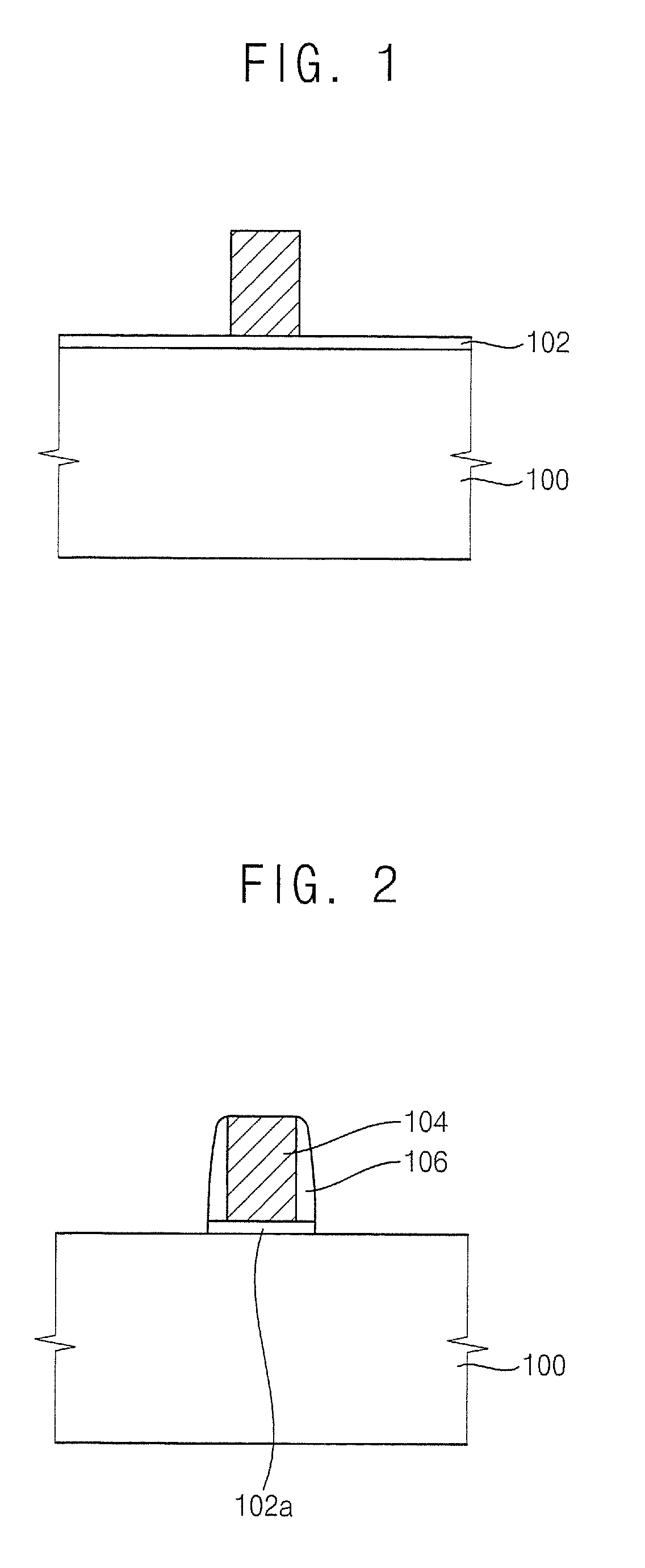
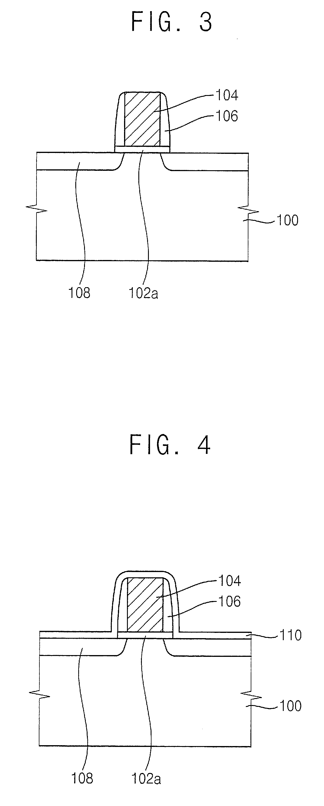
In some methods of manufacturing transistors, a gate electrode and a gate insulation layer pattern are stacked on a substrate. Impurity regions are formed at portions of the substrate that are adjacent to the gate electrode by implanting Group III impurities into the portions of the substrate. A diffusion preventing layer is formed on the substrate and covering the gate electrode. A nitride layer is formed on the diffusion preventing layer. The substrate is thermally treated to form a strained silicon region in the substrate between the impurity regions and to activate the impurities in the impurity regions. A high performance PMOS transistor and/or CMOS transistor may thereby be manufactured on the substrate.

Description

CROSS-REFERENCE TO RELATED APPLICATIONS[0001]This application claims priority under 35 U.S.C. § 119 to Korean Patent Application No. 10-2007-0045314 filed on May 10, 2007 and Korean Patent Application No. 10-2007-0059704 filed on Jun. 19, 2007, the entire contents of which are herein incorporated by reference in their entireties.BACKGROUND OF THE INVENTION[0002]1. Field of the Invention[0003]The present invention relates to methods of manufacturing transistors and, more particularly, to methods of manufacturing metal oxide semiconductor (MOS) transistors.[0004]2. Description of the Related Art[0005]Semiconductor devices have rapidly developed as information-processing circuits, such as a processors, and are being incorporated into more diverse types of electrical and electronic apparatuses. Semiconductor devices are increasingly being required to provide higher response speeds and greater storage capacity. To satisfy these requirements, manufacturing technologies are continuing to b...

Claims


Application Information

Patent Timeline
IPC IPC(8): H01L21/02
CPCH01L21/823807H01L29/7843H01L27/092
Inventor SHIN, DONG-SUKLEE, JOO-WONKIM, TAE-GYUN
Owner SAMSUNG ELECTRONICS CO LTD
Why Eureka
Try Eureka