Through electrode, manufacturing method thereof, and semiconductor device and manufacturing method thereof

Active Publication Date: 2016-11-03
NAT INST OF ADVANCED IND SCI & TECH
View PDF6 Cites 4 Cited by
  • Summary
  • Abstract
  • Description
  • Claims
  • Application Information

AI Technical Summary

Benefits of technology

[0009]In view of such background, an alternative insulating film has been demanded as a side-wall insulating film, instead of a silicon oxide film, and an organic low-dielectric constant material is considered theoretically as its candidate. If a side-wall insulating film made of an organic low-dielectric constant material can be formed at low-temperature process, the problem about thermomechanical reliability can be solved and capacitive coupling also can be suppressed, which therefore can suppress signal delay, power consumption and crosstalk and can improve the electrical characteristics.
[0010]However such a practically available organ

Problems solved by technology

However when silicon oxide is used as a side-wall insulating film to coat the side of a conductive layer of a through electrode, high-temperature process is required to coat the inner wall of a through hole.
A through electrode subjected to high-temperature process, however, has a problem of having poor thermomechanical reliability.
High-temperature process performed to form such a barrier lay

Method used


Image

  • Through electrode, manufacturing method thereof, and semiconductor device and manufacturing method thereof
  • Through electrode, manufacturing method thereof, and semiconductor device and manufacturing method thereof
  • Through electrode, manufacturing method thereof, and semiconductor device and manufacturing method thereof

Examples


Embodiment Construction

[0030]The following describes embodiments of the present invention in details. Referring now to the drawings, one embodiment of the present invention is described below. In the drawings, the same reference numerals are assigned to the same elements, and their duplicated descriptions are omitted. The positional relationship, such as above, below, left and right, in the descriptions is based on the positional relationship in the drawings unless otherwise specified. The dimensions and proportions in the drawings are not limited to those illustrated in the drawings. The following embodiment is just illustration to explain the present invention, which is not intended to limit the present invention to it. Further, the present invention is susceptible to various modifications without deviating from the gist thereof.

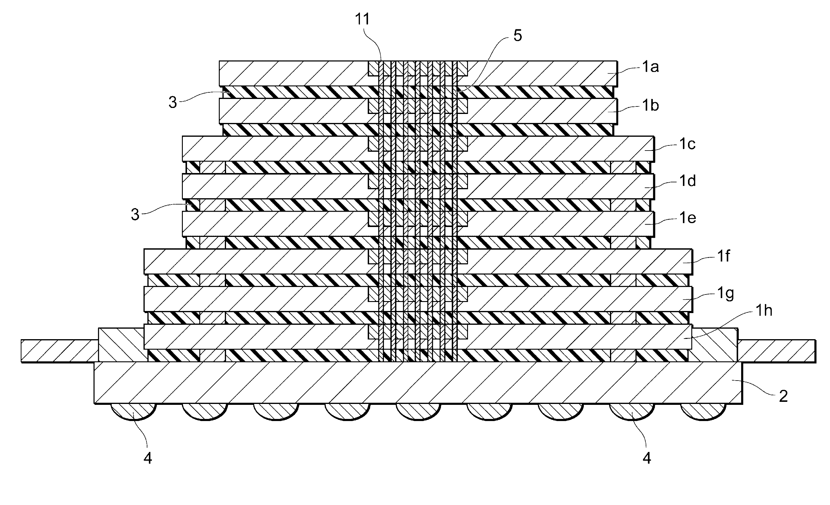
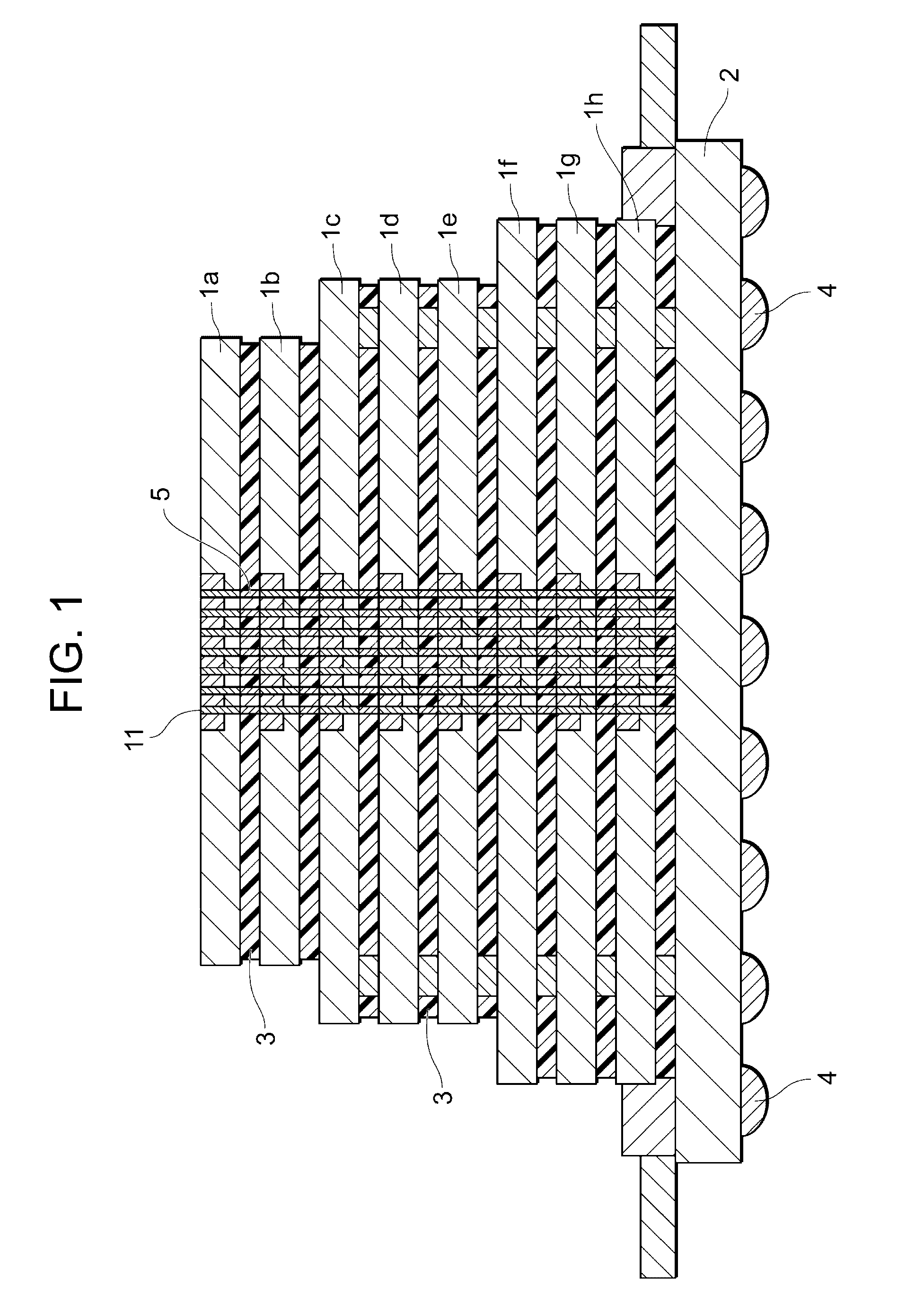
[0031]FIG. 1 is a cross-sectional view illustrating an exemplary schematic configuration of a three-dimensional stacked device, including a through electrode according to the pr...


PUM


Abstract

Provided are a through electrode including an organic side-wall insulating film, capable of eliminating a barrier layer and achieving satisfactory mechanical reliability and electrical reliability and a manufacturing method thereof, and a semiconductor device and a manufacturing method thereof. According to one aspect of the present invention, a through electrode disposed in a semiconductor substrate is provided, including: a copper layer in the semiconductor substrate; and a side-wall insulating film that is disposed between the copper layer and the semiconductor substrate so as to be in contact with the copper layer and the semiconductor substrate, the side-wall insulating film being represented by the following chemical formula (1).

Description

CROSS REFERENCE TO RELATED APPLICATIONS[0001]This application claims the benefit under 35 U.S.C. §119(a) of Japanese Patent Application No. 2015-093196, filed on Apr. 30, 2015, the entire disclosure of which is incorporated herein by reference in its entirety.BACKGROUND OF THE INVENTION[0002]1. Field of the Invention[0003]The present invention relates to a through electrode used in a three-dimensional integrated circuit and a manufacturing method thereof, and a semiconductor device and a manufacturing method thereof.[0004]2. Background Art[0005]Along with demands for more compact portable and wireless electronic devices, the development of finer and denser integrated circuits has been promoted to be used for micro-electronics in the next-generation. As a method to connect electronic devices mutually, three-dimensional packaging technology currently attracts attention. A through electrode, such as a through-silicon via (TSV), is one of the techniques to implement three-dimensional pa...

Claims


Application Information

Patent Timeline
IPC IPC(8): H01L23/48H01L21/288H01L21/02H01L23/532H01L21/768
CPCH01L23/481H01L23/53228H01L21/76898H01L21/288H01L21/76831H01L21/02118H01L23/5329H01L24/05H01L24/13H01L24/16H01L24/17H01L24/32H01L25/0657H01L25/50H01L2224/05647H01L2224/0569H01L2224/13025H01L2224/131H01L2224/13111H01L2224/13113H01L2224/13116H01L2224/13139H01L2224/13144H01L2224/13147H01L2224/13155H01L2224/16145H01L2224/16146H01L2224/16227H01L2224/1703H01L2224/17181H01L2224/2919H01L2224/32145H01L2224/32225H01L2224/33181H01L2224/73204H01L2225/06541H01L2225/06575H01L2924/15311H01L2924/00014H01L2924/014H01L2924/00H01L2224/16225H01L2924/0105H01L2924/01047H01L2924/01079H01L2924/01083H01L2924/06H01L2924/01029H01L2924/01082
Inventor AOYAGI, MASAHIROBUI, TUNG THANHWATANABE, NAOYAKATO, FUMIKIKIKUCHI, KATSUYA
Owner NAT INST OF ADVANCED IND SCI & TECH
Why Eureka
Try Eureka