Method for fabricating a capacitor

Inactive Publication Date: 2003-02-27
SK HYNIX INC
View PDF0 Cites 10 Cited by
  • Summary
  • Abstract
  • Description
  • Claims
  • Application Information

AI Technical Summary

Benefits of technology

0015] A method for fabricating a capacitor is disclosed which improves the electrical charac

Problems solved by technology

However, a complicated process is required to form the storage electrode into the 3-D structure so that fabrication costs increase and process efficiency decreases.
Also, when high dielectric materials are used, it is difficult to maintain the oxygen stoichiometry.
As a result, current leakage increases.
Because noble metals are very stable against an etching process and are etched by a dry etching technique, such as a sputtering technique or the like, there is a problem in that it is difficult t

Method used


Image

  • Method for fabricating a capacitor
  • Method for fabricating a capacitor
  • Method for fabricating a capacitor

Examples


Example

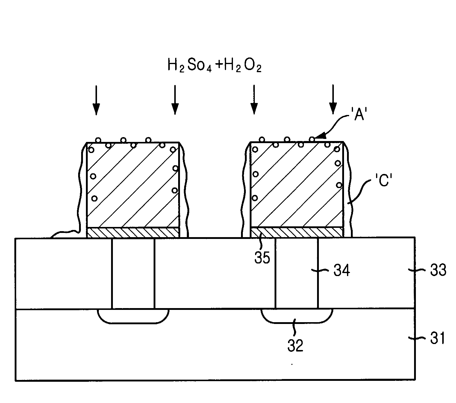
[0024] Hereinafter, the disclosed methods for fabricating capacitors in semiconductor devices will be described in detail referring to the accompanying drawings.

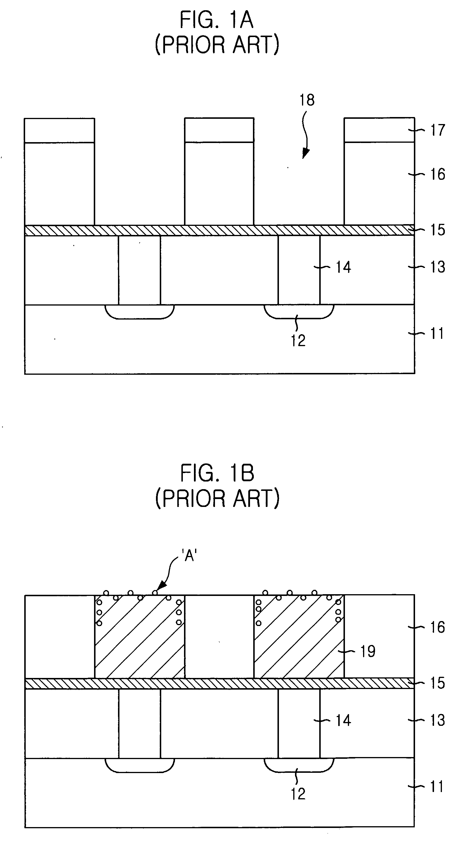
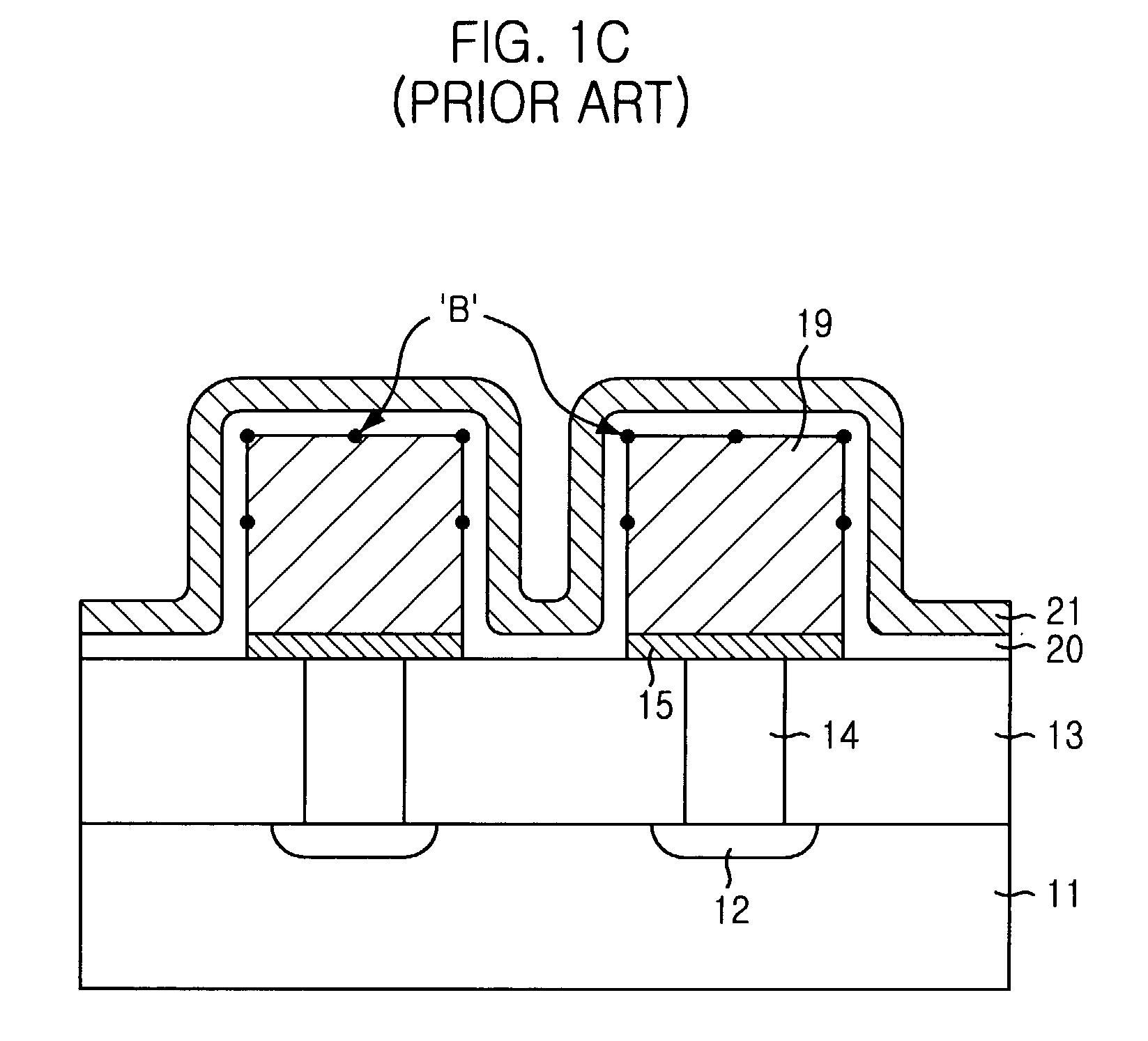
[0025] FIGS. 2A to 2D are cross-sectional views illustrating a fabricating capacitor according to one disclosed method.

[0026] Referring to FIG. 2A, an interlayer insulating layer 33 is formed on a semiconductor substrate 31 including a wordline (not shown) and a source / drain 32. The interlayer insulating layer 33 is formed with a material selected from a group consisting of phospho silicate glass (PSG), boro phospho silicate glass (BPSG), high density plasma (HDP) oxide, undoped silicate glass (USG), tetra ethyl ortho silicate (TEOS), advanced planarization layer (APL) oxide, spin on glass (SOG), flowfill and combinations thereof.

[0027] When considering a loss and an etching selection ratio of the interlayer insulating layer 33, a layer of a nitride layer family can be formed thereon by the CVD technique at a thickness rangi...


PUM


Abstract

Disclosed is a method for fabricating a capacitor, comprising the steps of forming a bottom electrode on the semiconductor substrate by an electro chemical deposition (ECD) technique, performing a wet-cleaning process for removing impurities of a surface of the bottom electrode, forming a dielectric layer on the bottom electrode and forming a top electrode on the dielectric layer.

Description

[0001] A method for fabricating a capacitor is disclosed, and more particularly, a method for fabricating a capacitor capable for reducing a current leakage is disclosed.[0002] A capacitance of a capacitor in a semiconductor device is represented as .di-elect cons.A / d, where `.di-elect cons.` represents a dielectric constant, `A` represents a surface area and `d` represents a thickness of a dielectric layer. That is, the capacitance is proportioned to a surface area of a storage electrode and a dielectric constant of a dielectric material.[0003] As a semiconductor device is highly integrated, in order to obtain a desired capacitance for a reliable operation thereof, the storage electrode is formed into a three-dimensional (3-D) structure to increase the surface area and high dielectric materials, such as BaTiO.sub.3, SrTiO.sub.3 or the like, has been used in the fabrication of the electrode. However, a complicated process is required to form the storage electrode into the 3-D struct...

Claims


Application Information

Patent Timeline
IPC IPC(8): H01L21/02H01L21/288H01L21/308H01L21/8242H01L27/108
CPCH01L21/2885H01L28/60H10B99/00
Inventor CHO, HO-JINCHOI, HYUNG-BOK
Owner SK HYNIX INC
Why Eureka
Try Eureka