Polycrystalline Silicon Rod For Zone Reflecting And A Process For The Production Thereof

a polycrystalline silicon and zone reflecting technology, applied in the direction of crystal growth process, synthetic resin layered products, record information storage, etc., can solve the problems of inability to use rods afflicted with cracks or high thermal strains, the yield of finished polycrystalline rods is significantly less than 100%, and the production cost of polycrystalline rods is reduced. , to achieve the effect of reducing the production cost of polycrystalline rods, high yield and cost saving

Active Publication Date: 2008-11-20
WACKER CHEM GMBH
View PDF10 Cites 53 Cited by
  • Summary
  • Abstract
  • Description
  • Claims
  • Application Information

AI Technical Summary

Benefits of technology

[0017]An object of the invention is to provide polycrystalline silicon rods with high yield during the production of thick polycrystalline silicon rods having a diameter of greater than 120 mm for FZ applications, and to counteract the frequent formation of defects during the refining of the polycrystalline silicon rods to form FZ single crystals having a large diameter. A further aim of the invention is to reduce the production costs of polycrystalline rods by using more cost-effective polycrystalline filament rods in contrast to the monocrystalline filament rods described in the prior art which are produced in a complicated manner and are therefore expensive.

Problems solved by technology

Since the feet and the bridges of the U-shaped bodies cannot be used for FZ refining, the yield of the finished polycrystalline rods is significantly less than 100%.
During the production of polycrystalline Si rods having a thick diameter it is often observed that the rods have cracks or break in the course of removal from the reactor or in the course of mechanical processing to form finished rods.
The rods afflicted with cracks or high thermal strains cannot be used for mechanical processing to form the finished polycrystalline rods and for subsequent production of the monocrystalline rods by means of the FZ process.
If the rods withstand this treatment, they can result in serious consequences during zone refining.
Since the rods are heated up to the melting point in this process, the cracked or thermally strained rods can shatter on account of additional thermal stresses.
This leads to material and time losses as a result of the termination of the refining process.
Furthermore, the refining apparatus can also be damaged by the rod pieces that have splintered off.
Therefore, cracked and thermally strained polycrystalline silicon rods have to be sorted out prior to refining or be shortened to the defect site.
This material exclusion once again reduces the yield.
However, the process can only avoid the formation of those cracks which arise only after the end of the deposition during the cooling down of the rods.
However, cracks can already form during the deposition in the rods.
However, this process requires monocrystalline thin rods of square cross section in a special orientation where the longitudinal axis points in the direction, the production of which is very complicated and expensive.
Moreover, this process requires a high temperature and low deposition rate.
The lower deposition rate means that this deposition process has lower economic viability.
The high deposition temperature causes high thermal stresses and thus leads to cracked rods.
However, the methods described cannot prevent the formation of disturbing coarse monocrystalline inclusions.
Moreover, the processes proposed lead to high thermal stresses in the case of thick polycrystalline silicon rods having a diameter of greater than 120 mm, such that the crack-free yield of the finished rods after mechanical processing is very low, usually lower than 40%.
These rings in the polycrystalline Si rods disturb the FZ refining process and cause defects in the monocrystalline FZ rod.
All of the known methods from the prior art yield either very thin polycrystalline rods or thicker rods having stresses which, upon cooling down or during further processing, lead to defects through to the total unusability of the rod.

Method used


Image

  • Polycrystalline Silicon Rod For Zone Reflecting And A Process For The Production Thereof
  • Polycrystalline Silicon Rod For Zone Reflecting And A Process For The Production Thereof
  • Polycrystalline Silicon Rod For Zone Reflecting And A Process For The Production Thereof

Examples


example 4

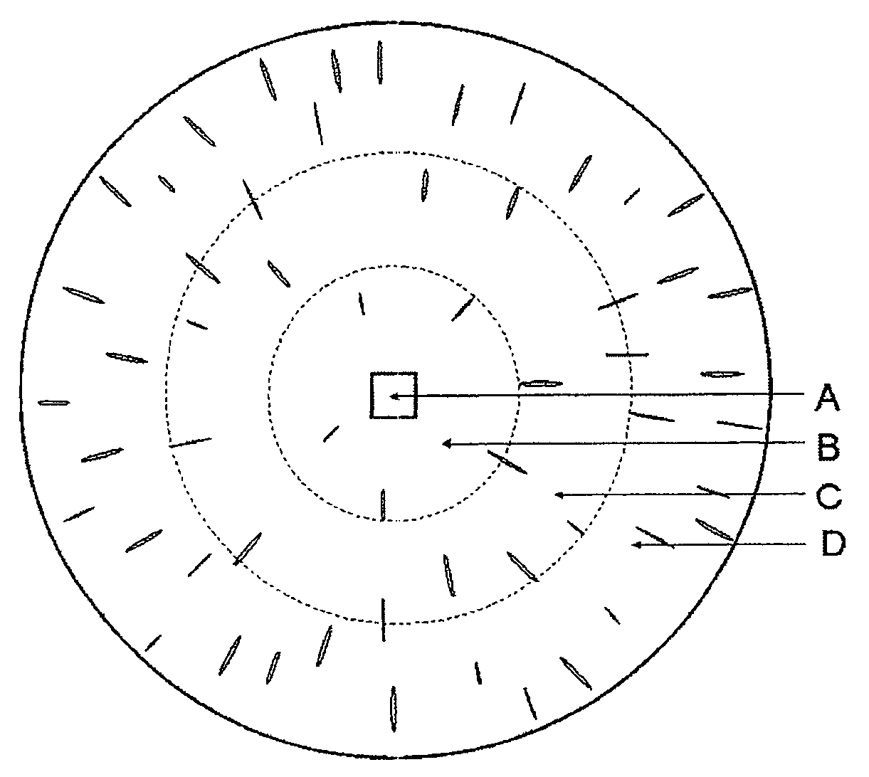
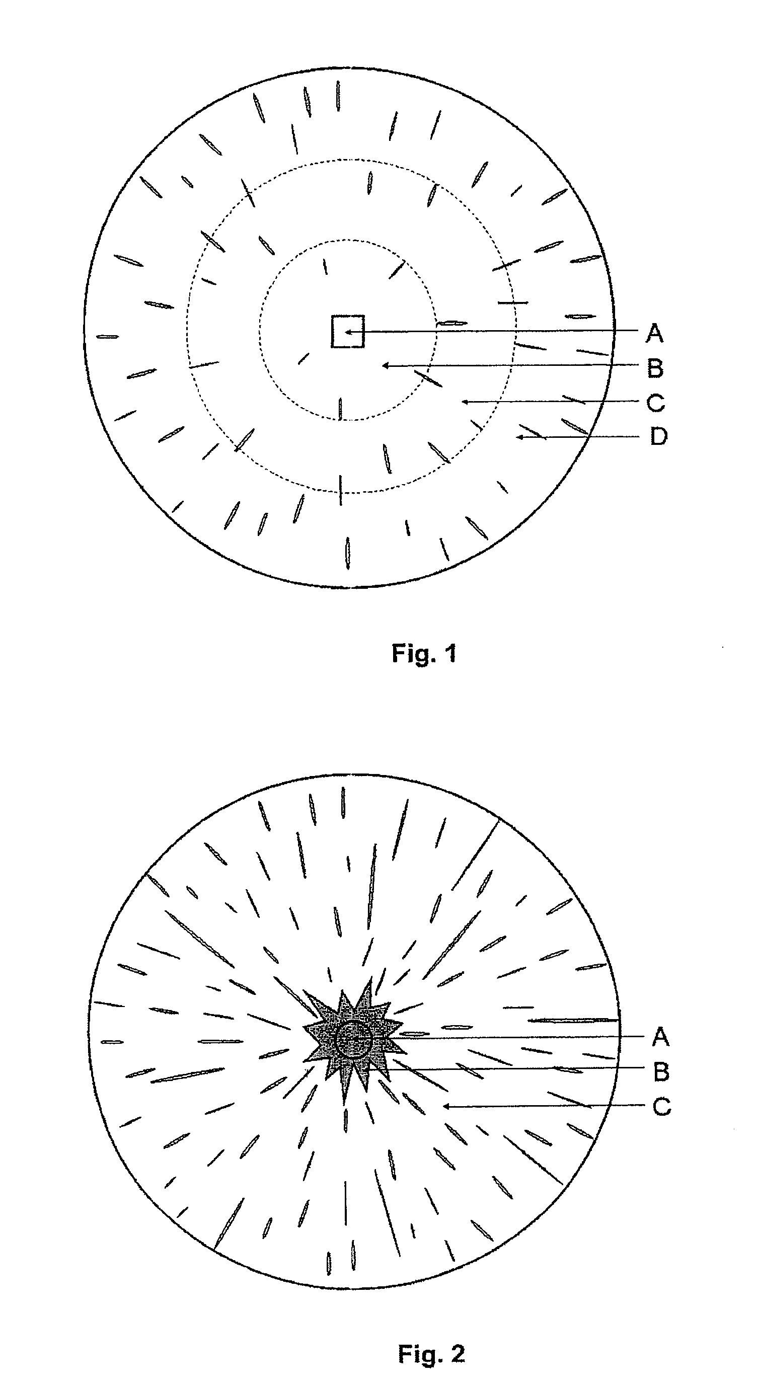
[0060]The polycrystalline silicon rods described in this example were deposited according to the present invention. Trichlorosilane was used as silicon-containing component of the reaction gas. The polycrystalline Si thin rods (square cross section, edge length 8 mm) were used as carrier bodies. Firstly, the deposition was carried out at 1050° C. with a gas mixture having a TCS fraction of 20%. The deposition rate was 0.35 mm / h in this step, as also throughout the deposition time. After the rods had reached the diameter of 60 mm, the rod temperature was slowly lowered to 990° C. and at the same time the TCS fraction was increased to 40%. The change took place slowly (“fluidly”), such that it was completed only when the rod reached the diameter of 102 mm (after 60 hours). The deposition was then continued under these conditions until the rods reached the diameter of 150 mm. After removal from the reactor, the rods, having an average crack-free yield of 75% could be processed for the ...


PUM

PropertyMeasurementUnit
lengthaaaaaaaaaa
widthaaaaaaaaaa
widthaaaaaaaaaa

Abstract

The invention relates to a polysilicon rod for FZ applications obtainable by deposition of high-purity silicon from a silicon-containing reaction gas, which has been thermally decomposed or reduced by hydrogen, on a filament rod. The polysilicon rod contains, surrounding the filament rod, an inner zone having but few needle crystals, small in size, an outer zone having a relatively small amount of larger needle crystals, and a smooth transition zone between the inner and outer zones. The polysilicon rods are obtained in high yield and can be refined in one pass in an FZ process.

Description

BACKGROUND OF THE INVENTION[0001]1. Field of the Invention[0002]The invention relates to a rod composed of polycrystalline silicon for further use in the production of a monocrystalline rod by means of a floating zone process (FZ process), and a process for the production thereof.[0003]2. Background Art[0004]High-purity polycrystalline silicon (polysilicon) serves as a starting material for the production of monocrystalline silicon for semiconductors according to the Czochralski process (CZ) or the floating zone process (FZ) and for the production of solar cells for photovoltaics.[0005]Polycrystalline silicon rods are generally produced according to the Siemens process. In this case, a silicon-containing reaction gas is thermally decomposed or reduced by hydrogen and deposited as high-purity silicon on thin filament rods made of silicon, so-called thin rods or cores. Halosilanes, such as trichlorosilane, for example, are predominantly used as the silicon-containing component of the ...

Claims


Application Information

Patent Timeline
Patent Type & Authority Applications(United States)
IPC IPC(8): B32B5/00B32B5/16C23C14/00C01B33/02
CPCC01B33/035C23C16/24Y10T428/26C30B29/06C30B13/00
Inventor SOFIN, MIKHAILFREIHEIT, HANS-CHRISTOFKRAUS, HEINZ
Owner WACKER CHEM GMBH
Why Eureka
Try Eureka