Photodiode for Image Sensor and Method of Manufacturing the Same

a photodiode and image sensor technology, applied in the field of can solve the problems of low light absorption of silicon-based photodiodes for image sensors, difficult miniaturization of elements, and inability to perform ar coating with respect to all visible light required by visible light image sensors, etc., to achieve the effect of increasing the absorption of light, reducing the reflection of light, and increasing the length of the path

Inactive Publication Date: 2008-11-27
SILICONFILE TECH INC
View PDF1 Cites 17 Cited by
  • Summary
  • Abstract
  • Description
  • Claims
  • Application Information

AI Technical Summary

Benefits of technology

[0016]The present invention provide a photodiode capable of reducing reflection of light regardless of an incident angle and a wavelength of the light incident onto a photodiode surface ...

Problems solved by technology

However, the silicon-based photodiode for the image sensor has a low absorptance of light.
Since a photodiode having a large area is required for a sufficient signal due to a low absorptance of light, it is difficult to miniaturize elements.
Since a wavelength used in the visible light image sensor ranges from 400 nm to 700 nm, the reflectances with respect to red and blue light are large, it ...

Method used


Image

  • Photodiode for Image Sensor and Method of Manufacturing the Same
  • Photodiode for Image Sensor and Method of Manufacturing the Same
  • Photodiode for Image Sensor and Method of Manufacturing the Same

Examples


Embodiment Construction

[0025]Hereinafter, the present will be described in detail with reference to accompanying drawings.

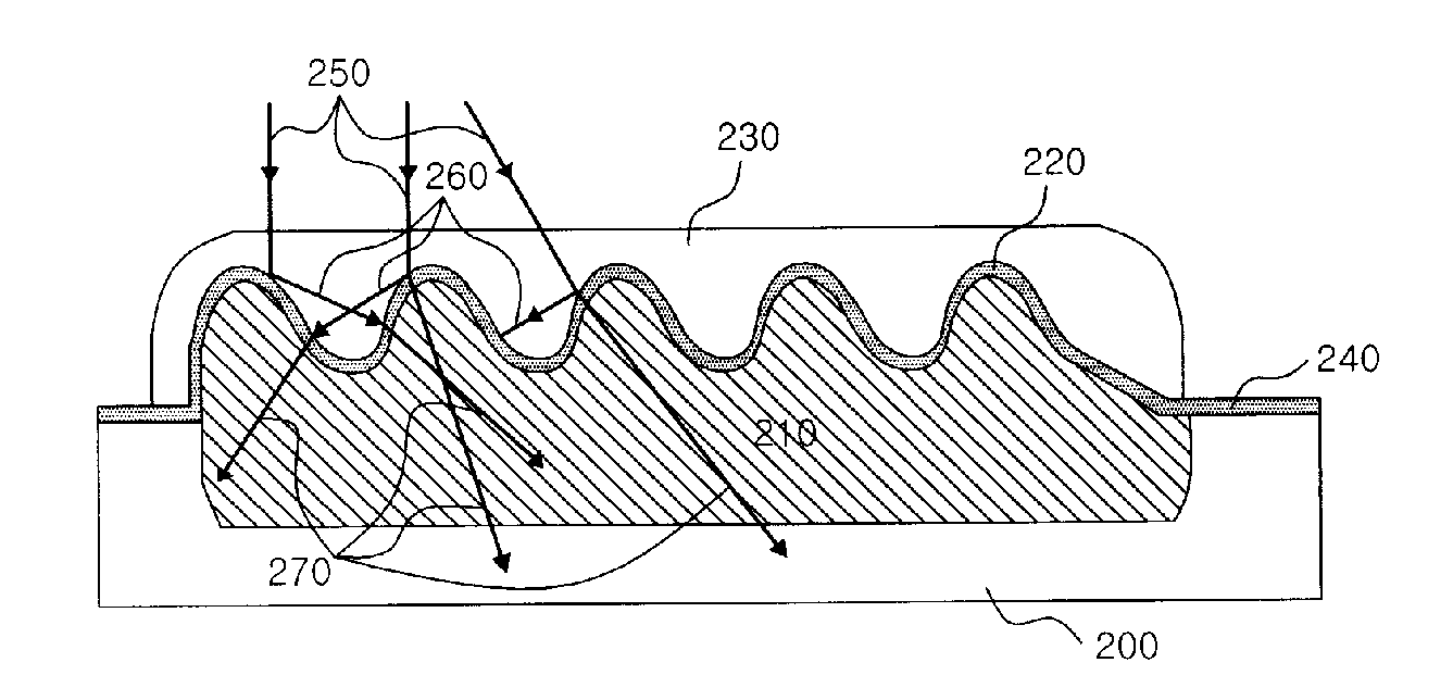
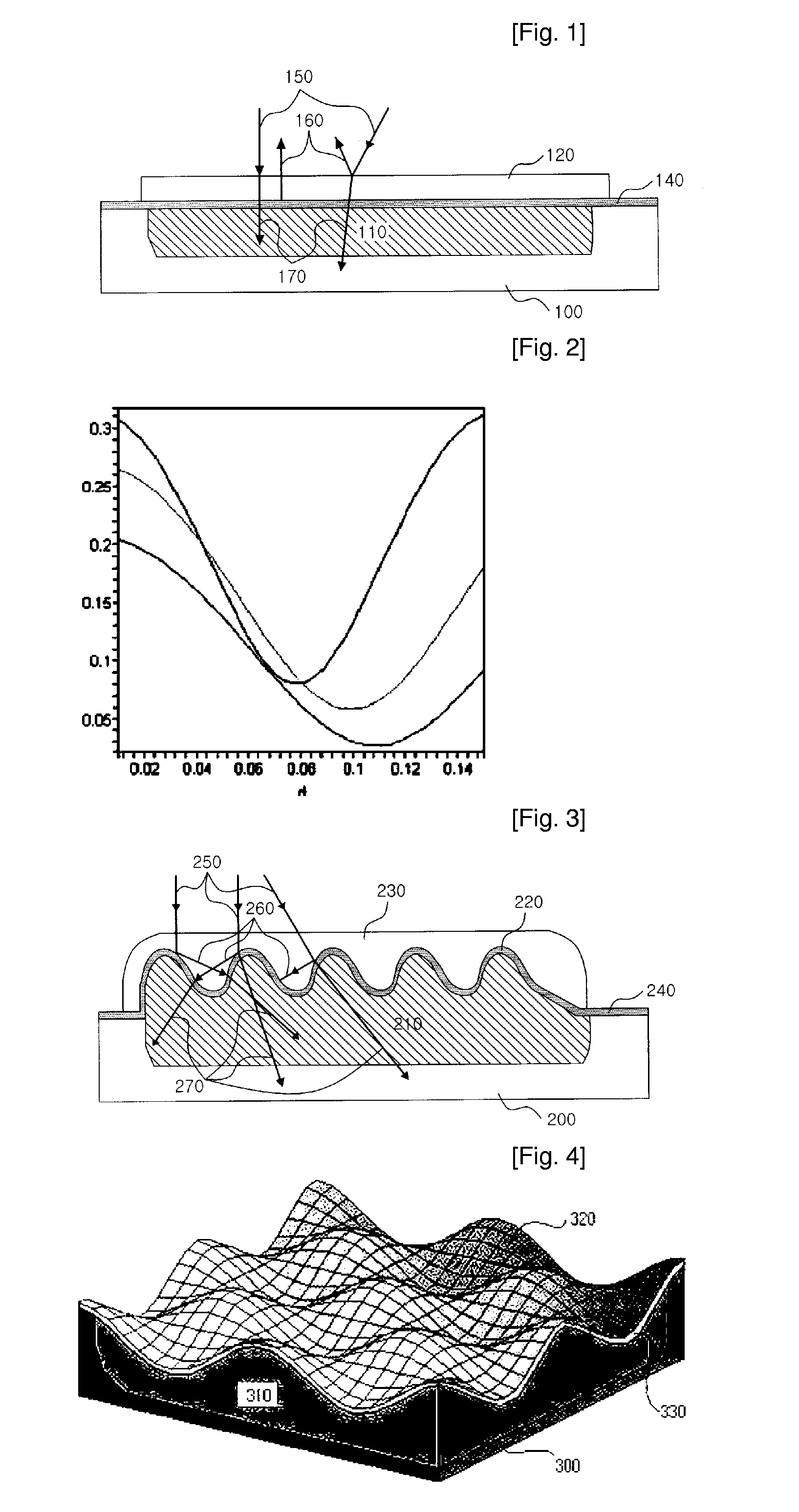
[0026]FIG. 3 schematically illustrates a cross sectional view of a silicon photodiode for an image sensor according to an embodiment of the present invention. The photodiode for the image sensor includes a photodiode region 210, a silicon concavo-convex surface 220, a silicon oxide layer 230, and a doped region 240.

[0027]The silicon concavo-convex surface 220 with a nano-thickness is formed on the photodiode region 210 formed on silicon substrate 200.

[0028]The doped region 240 for suppressing a leakage current by separating the photodiode region 210 from the surface of the photodiode is formed on the silicon concavo-convex surface 220 by doping.

[0029]The optically transmissive silicon oxide layer 230 is formed on the doped region 240.

[0030]A surface of a photodiode according to an embodiment of the present invention includes the silicon concavo-convex surface 220 with a nano-thickness ...


PUM


Abstract

A photodiode for an image sensor capable of reducing reflection of light incident onto the photodiode and effectively absorbing transmitted light and a method of manufacturing the same are provided. In the photodiode for the image sensor, a silicon concavo-convex surface with a nano-thickness is formed by forming silicon oxide (SiO, x=0.5-1.5) layer on a silicon substrate and treating the silicon oxide layer with heat. A photodiode region is formed under the silicon layer having convexes and concaves. In this case, light absorptance increases because light reflected on the silicon concavo-convex surface is reincident onto another convex or concave. Therefore, an effective depth of the photodiode is larger than that of a planar photodiode, and accordingly, quantum efficiency of the photodiode increases.

Description

TECHNICAL FIELD[0001]The present invention relates to a photodiode for an image sensor, and more particularly to a photodiode which has a structure capable of reducing light reflected on a silicon-based photodiode surface and increasing light absorbed in the photodiode and a method of manufacturing the same.BACKGROUND ART[0002]An image sensor is used for measuring intensity of light. In general, the image sensor includes a plurality of photodiodes. The photodiodes are manufactured on the basis of silicon.[0003]However, the silicon-based photodiode for the image sensor has a low absorptance of light. Accordingly, for example, a transmission depth is large in a red wavelength range.[0004]A photo-sensor region is required to be deep due to the large transmission depth, thereby generating a crosstalk. Since a photodiode having a large area is required for a sufficient signal due to a low absorptance of light, it is difficult to miniaturize elements. Light reflected on a silicon surface ...

Claims


Application Information

Patent Timeline
IPC IPC(8): H01L31/0224
CPCH01L27/1462H01L27/14685H01L31/0236Y02E10/50H01L31/02363H01L27/146B82Y20/00
Inventor LEE, BYOUNG SU
Owner SILICONFILE TECH INC
Why Eureka
Try Eureka