

Semiconductor integrated circuit device having fail-safe mode and memory control method
- Summary
- Abstract
- Description
- Claims
- Application Information
AI Technical Summary
Benefits of technology
Problems solved by technology
Method used
Image

Examples
Embodiment Construction
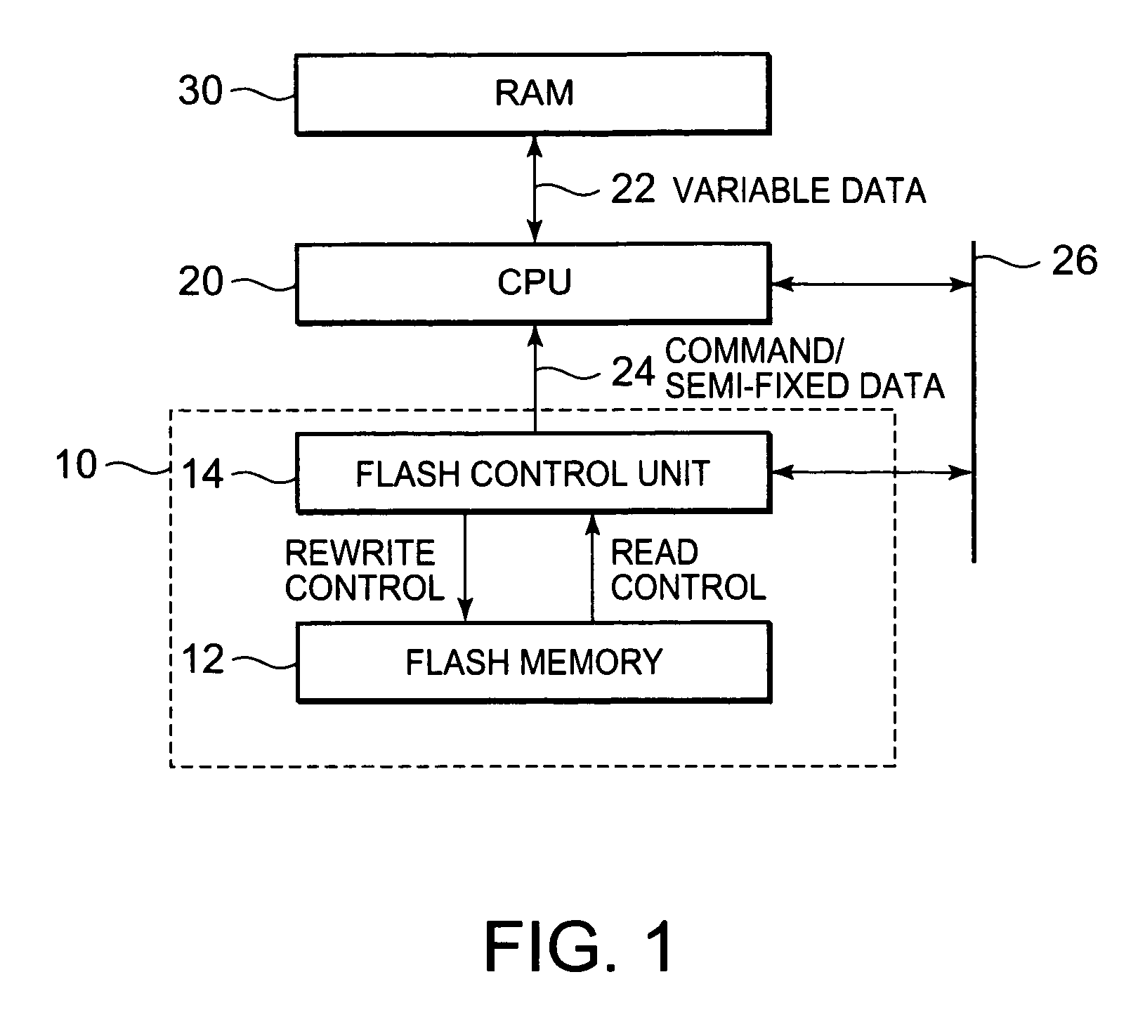
[0033]FIG. 1 shows the structure of the microprocessor of an exemplary embodiment of this invention. The microprocessor contains a CPU (central processing unit) 20, a RAM (random access memory) 30, and a flash unit 10. The CPU 20 loads (read out) commands from the flash unit 10 by way of the bus 24, loads data for storage onto the RAM 30 and writes data such as processed data into the RAM 30 via the bus 22. Data that must be retained even if the power is not supplied is stored in the flash unit 10. This data is loaded and processed. The flash unit 10 contains a flash memory 12 for retaining data and a flash control unit 14 for controlling the reading and controlling the writing of the flash memory 12. Data stored in the flash unit 10 can be written and read out by way of the peripheral bus 26.
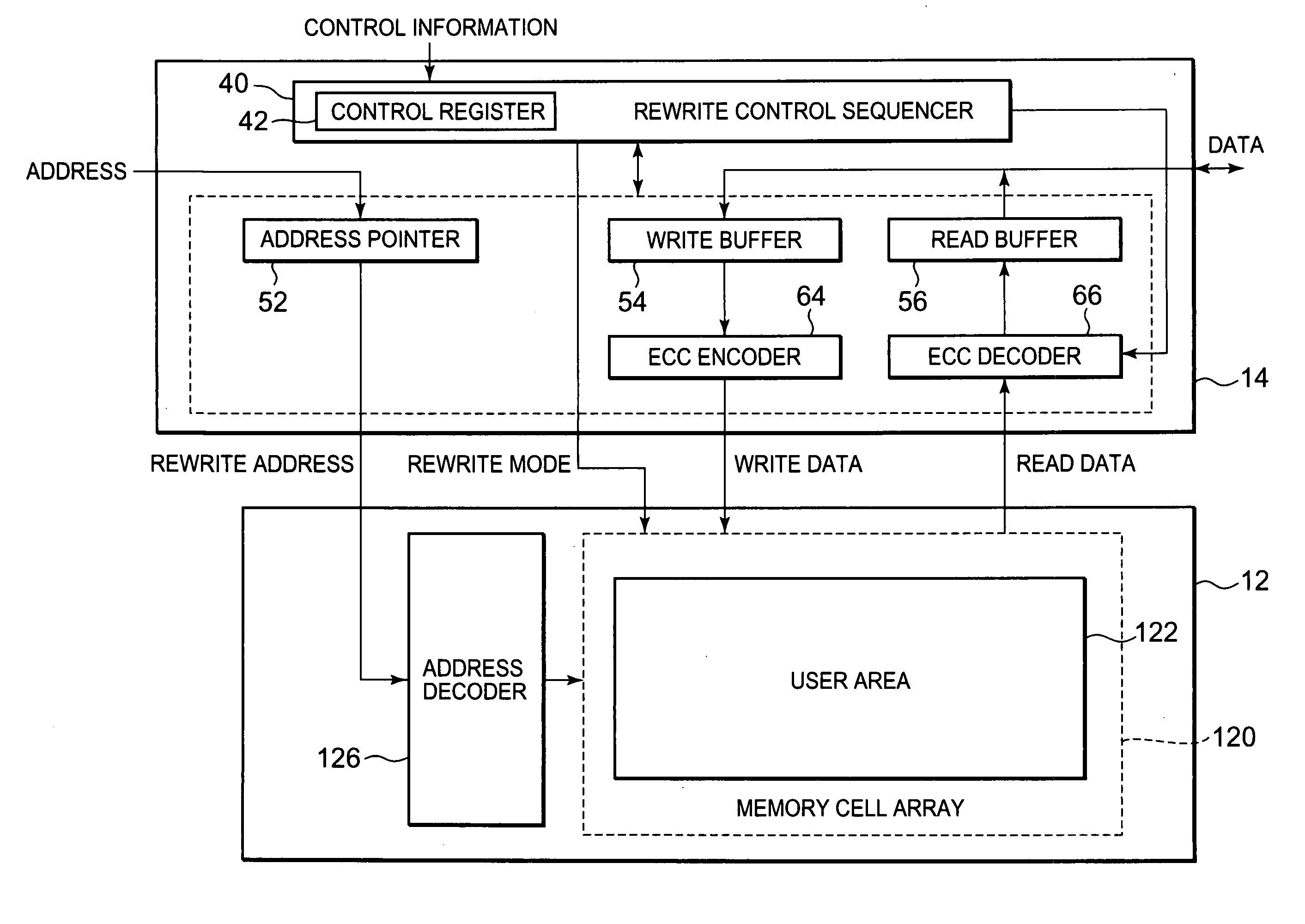
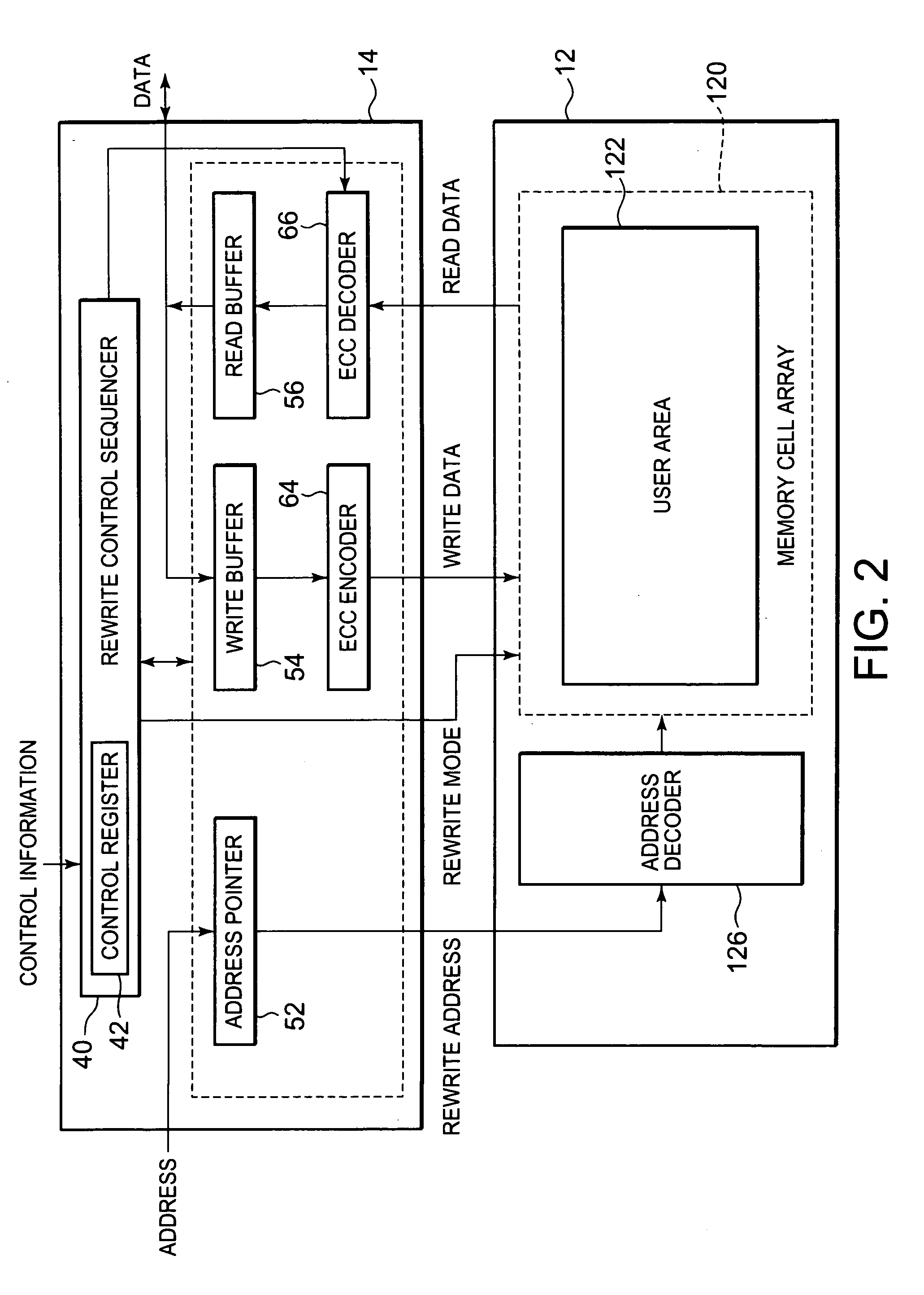
[0034]FIG. 2 shows the structure of the flash unit 10 of the first embodiment of this invention. This figure shows the memory control method implemented by software in the first embodiment. The...
PUM
 Abstract
Description
Claims
Application Information