
CMOS image sensor and pixel of the same

a technology of metal oxidesemiconductor and image sensor, which is applied in the field of solid-state image sensors, can solve the problems that the typical transfer gate transistors have limitations that are difficult to overcome, and achieve the effects of low dark current, high charge transfer efficiency, and good blooming control

Active Publication Date: 2008-12-04
INTELLECTUAL VENTURES II
View PDF4 Cites 21 Cited by
  • Summary
  • Abstract
  • Description
  • Claims
  • Application Information

AI Technical Summary

Benefits of technology

[0022]Embodiments of the present invention are directed to provide a description of complementary metal-oxide-semiconductor (CMOS) image sensor having pixels that use pinned photodiodes and charge transfer transistors, wherein the charge transfer transistor has high charge transfer efficiency, good blooming control, and low dark current.

Problems solved by technology

However, it is still necessary to transfer charge from a photodiode onto a FD node using a charge transfer transistor in all of those designs.
Therefore, the typical transfer gate transistors have limitations that are difficult to overcome.

Method used


Image

  • CMOS image sensor and pixel of the same
  • CMOS image sensor and pixel of the same
  • CMOS image sensor and pixel of the same

Examples


Embodiment Construction

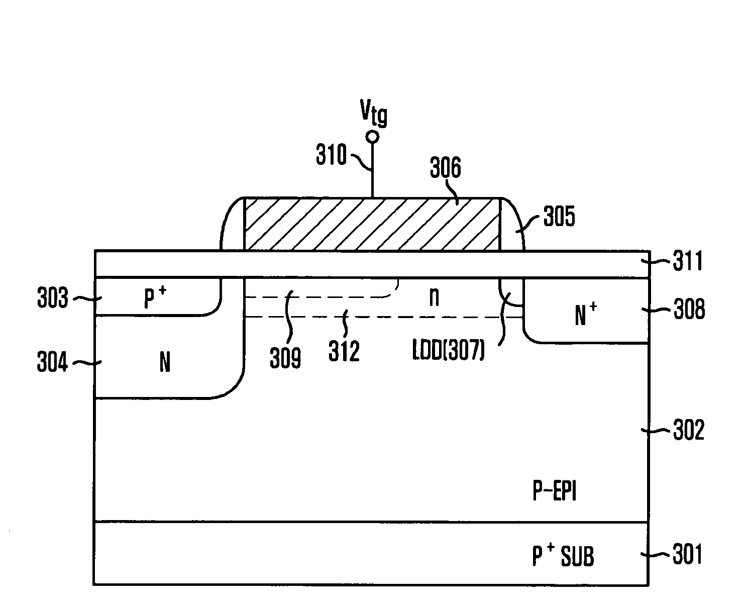
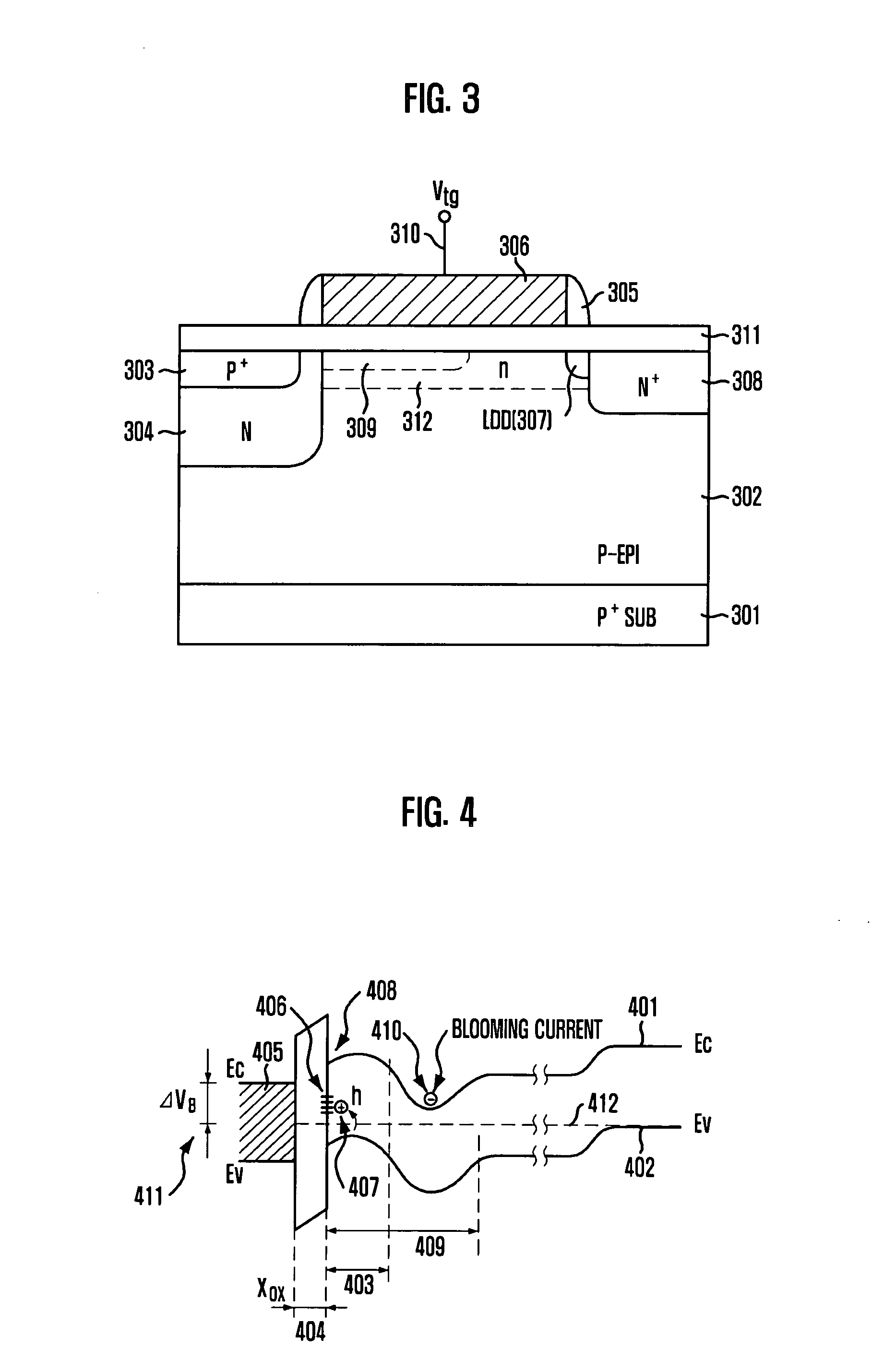
[0029]FIG. 3 illustrates a cross sectional view of a charge transfer transistor according to an embodiment of the present invention.

[0030]A substrate 301 includes an epitaxial layer doped with p+-type impurities. A p-type impurity doped epitaxial layer 302 is formed over the p+-type impurity doped substrate 301.

[0031]A pinned photodiode region including a p+-type impurity doped region 303 and a first n-type impurity doped region 304, a charge transfer gate 306 and a floating diffusion (FD) region 308 are formed over the p-type impurity doped epitaxial layer 302. The charge transfer gate 306 may include polysilicon. The charge transfer gate 306 is isolated from the substrate 301 by a gate insulation layer 311 formed by silicon dioxide or some other insulation layer. The transfer gate 306 may also include sidewall spacers 305.

[0032]The metal interconnection 310 of the charge transfer gate 306 to a driving signal source is shown only schematically. The charge transfer transistor may in...


PUM


Abstract

A pixel of an image sensor includes a gate insulation layer formed over a substrate doped with first-type impurities, a transfer gate formed over the gate insulation layer, a photodiode formed in the substrate at one side of the transfer gate, and a floating diffusion node formed in the substrate at the other side of the transfer gate, wherein the transfer gate has a negative bias during a charge integration cycle.

Description

CROSS-REFERENCE TO RELATED APPLICATIONS[0001]The present invention claims priority of Korean patent application number 10-2007-0053867 filed on Jun. 1, 2007, which is incorporated by reference in its entirety.BACKGROUND OF THE INVENTION[0002]The present invention relates to solid-state image sensors, and more particularly to a complementary metal-oxide-semiconductor (CMOS) image sensor having a pinned photodiode for light sensing and incorporating a charge transfer gate for transferring signal charge from the photodiode to a floating diffusion node. More specifically, the present invention relates to pixels using a correlated double sampling operation for minimizing kTC reset noise, incorporating blooming control therein, and having a very low dark current.[0003]The typical image sensors sense light by converting impinging photons into electrons that are integrated in sensor pixels. After completing an integration cycle, collected charge is converted into a voltage, which is supplie...

Claims


Application Information

Patent Timeline
Patent Type & Authority Applications(United States)
IPC IPC(8): H01L27/148H01L27/146H04N25/00
CPCH01L27/14609H01L27/14654H01L27/146
Inventor HYNECEK, JAROSLAVHAN, HYUNG-JUN
Owner INTELLECTUAL VENTURES II
Learn More