Projection objective and projection exposure apparatus for microlithography

Active Publication Date: 2008-12-04
CARL ZEISS SMT GMBH
View PDF15 Cites 23 Cited by
  • Summary
  • Abstract
  • Description
  • Claims
  • Application Information

AI Technical Summary

Benefits of technology

[0007]In some embodiments, the disclosure provides a projection objective having a low level of aberrations

Problems solved by technology

Energy absorption typically causes heating of the optical elements subject to the radiation.
However, lens heating may cause deterioration of optical properties in optical systems optimized for “cold condition” during operation.
While a compensation of lens heating effects through external manipulation devices may be possible where the lens heating is essentially uniform or rotationally symmetric on important optical elements, compensation may be difficult where non-uniform l

Method used


Image

  • Projection objective and projection exposure apparatus for microlithography
  • Projection objective and projection exposure apparatus for microlithography
  • Projection objective and projection exposure apparatus for microlithography

Examples


Embodiment Construction

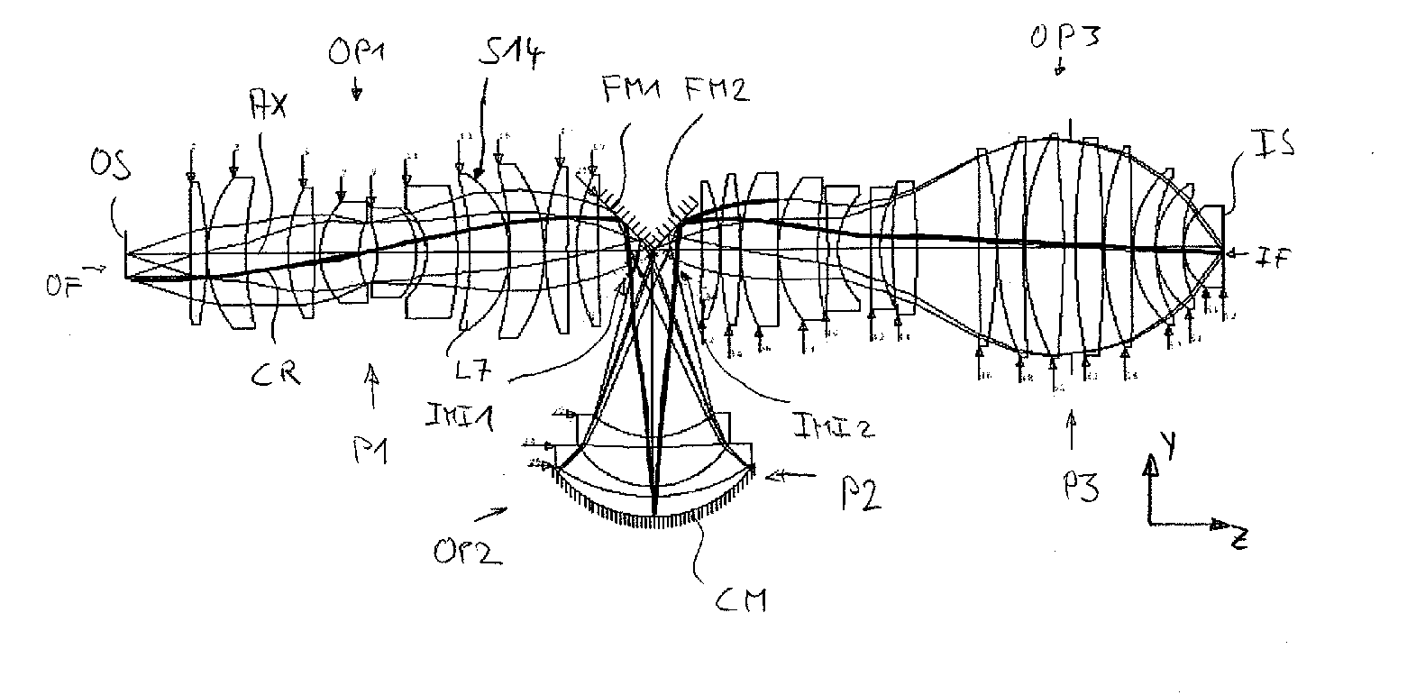
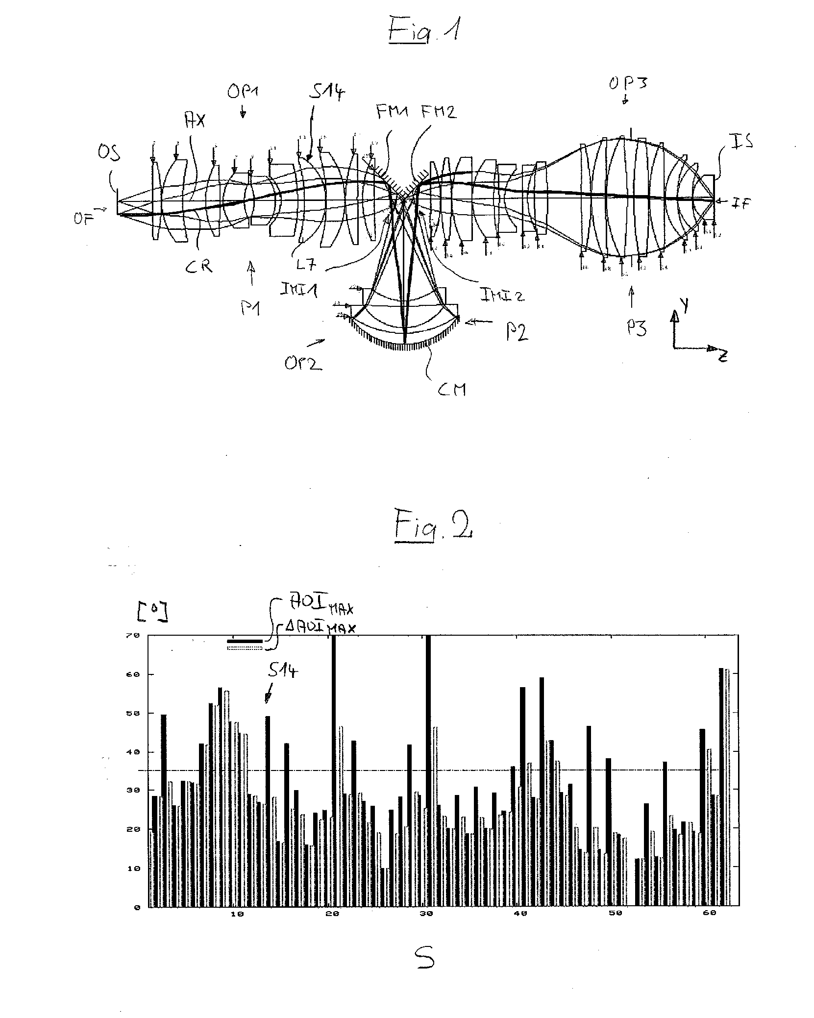
[0062]In the following description, the term “optical axis” refers to a straight line or a sequence of a straight-line segments passing through the centers of curvature of optical elements. The optical axis can be folded by folding mirrors (deflecting mirrors) such that angles are included between subsequent straight-line segments of the optical axis. In the examples presented below, the object is a mask (reticle) bearing the pattern of a layer of an integrated circuit or some other pattern, for example, a grating pattern. The image of the object is projected onto a wafer serving as a substrate that is coated with a layer of photoresist, although other types of substrates, such as components of liquid-crystal displays or substrates for optical gratings, are also feasible.

[0063]Where appropriate, corresponding features in the figures are designated with like or identical reference identifications to facilitate understanding.

[0064]A number of known projection objectives designed for i...


PUM


Abstract

Projection objective, projection exposure apparatuses and related systems and components are disclosed.

Description

CROSS-REFERENCE TO RELATED APPLICATION[0001]This application claims priority under 35 U.S.C. §119(e)(1) to U.S. Provisional Application No. 60 / 941,369, filed on Jun. 1, 2007, which is hereby incorporated by reference.FIELD[0002]The present disclosure relates to a projection objective and a projection exposure apparatus configured to be used in a microlithography process. The apparatus can be used to expose a radiation-sensitive substrate, arranged in the region of an image surface of the projection objective, with at least one image of pattern of a mask arranged in the region of an object surface of the projection objective. The present disclosure also relates to related components and methods.BACKGROUND[0003]Microlithographic projection exposure methods are used for fabricating semiconductor components and other finely structured components. Use is made of masks (reticles) that bear the pattern of a structure to be imaged, for example a line pattern of a layer of a semiconductor co...

Claims


Application Information

Patent Timeline
IPC IPC(8): G02B17/08G02B13/14G06F17/50
CPCG02B13/143G02B17/0812G02B17/0892G03F7/70225G03F7/70891
Inventor MUELLER, RALF
Owner CARL ZEISS SMT GMBH
Why Eureka
Try Eureka