Semiconductor apparatus and production method of the same

a semiconductor and production method technology, applied in the direction of semiconductor devices, electrical devices, transistors, etc., can solve the problems of fluctuation of the threshold voltage of the transistor, difficult floating body effect, etc., to achieve high integration, simple structure, and fine layout.

Inactive Publication Date: 2008-12-11
LONGITUDE LICENSING LTD
View PDF2 Cites 39 Cited by
  • Summary
  • Abstract
  • Description
  • Claims
  • Application Information

AI Technical Summary

Benefits of technology

[0030]In addition, in the semiconductor apparatus of the above-described aspect, each of the three-dimensional transistors has both a lower diffused layer leading portion and a gate electrode leading portion that are close to the first pillar. The three-dimensional transistors surrounded by the well layer constitute a module in a manner in which each of the three-dimensional transistors is arranged at a vertex of a hexagon that has a center at which the second pillar is set. Therefore, by using such a module as a unit, it is possible to constitute a transistor from multiple units, and it is possible to produce a semiconductor apparatus which is large and has a complicated structure.
[0031]In addition, in the semiconductor apparatus of the above-described aspect, the modules are arranged in a honeycomb state. Therefore, it is possible to achieve a closest packed structure, it is possible to achieve a fine layout, and it is possible to produce a further highly integrated semiconductor apparatus.
[0032]In addition, in the semiconductor apparatus production method of the above-described aspect, semiconductor apparatus includes steps of: forming a channel portion around each of multiple first pillars; forming diffused layers at an upper portion and a lower portion of the channel portion; forming each of multiple three-dimensional transistors by forming a gate terminal around the channel portion via a gate insulation film; and arranging the multiple three-dimensional transistors on a well area while surrounding a second pillar which is electrically conductive. In addition, the multiple three-dimensional transistors share the second pillar which is a single pillar, and the channel portions of the multiple three dimensional transistor...

Problems solved by technology

However, compared to a conventional planer transistor in which the electric potential or voltage of a channel portion is controlled by a substrate, in a constitution of a three-dimensional transistor shown in FIG. 14, even though the electric potential of the upper and lower diffused layers are controlled, the potential of a channel portion wh...

Method used


Image

  • Semiconductor apparatus and production method of the same
  • Semiconductor apparatus and production method of the same
  • Semiconductor apparatus and production method of the same

Examples


Embodiment Construction

[0056]Hereinafter, an embodiment which is an example of the present invention is explained in reference to the drawings.

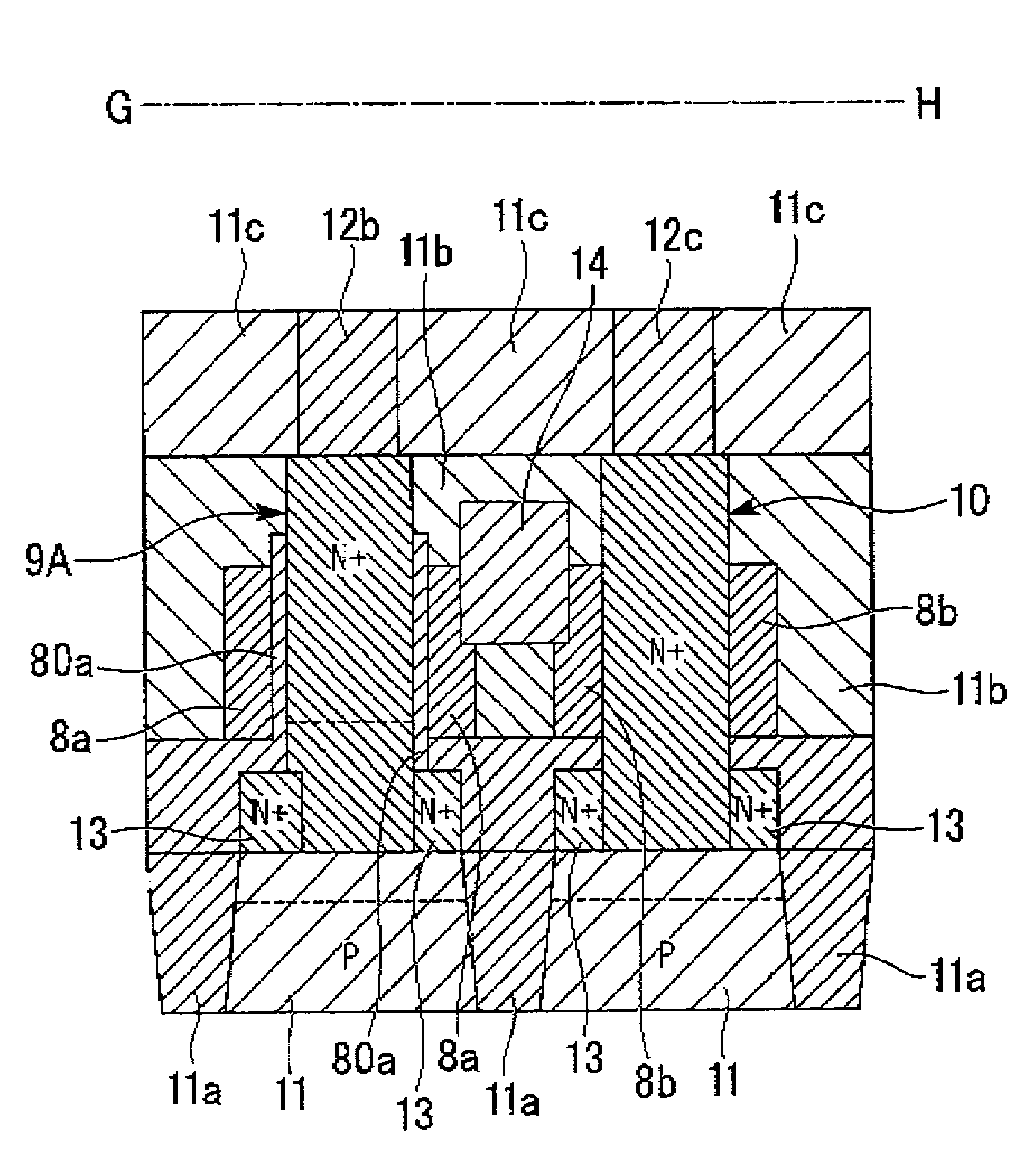
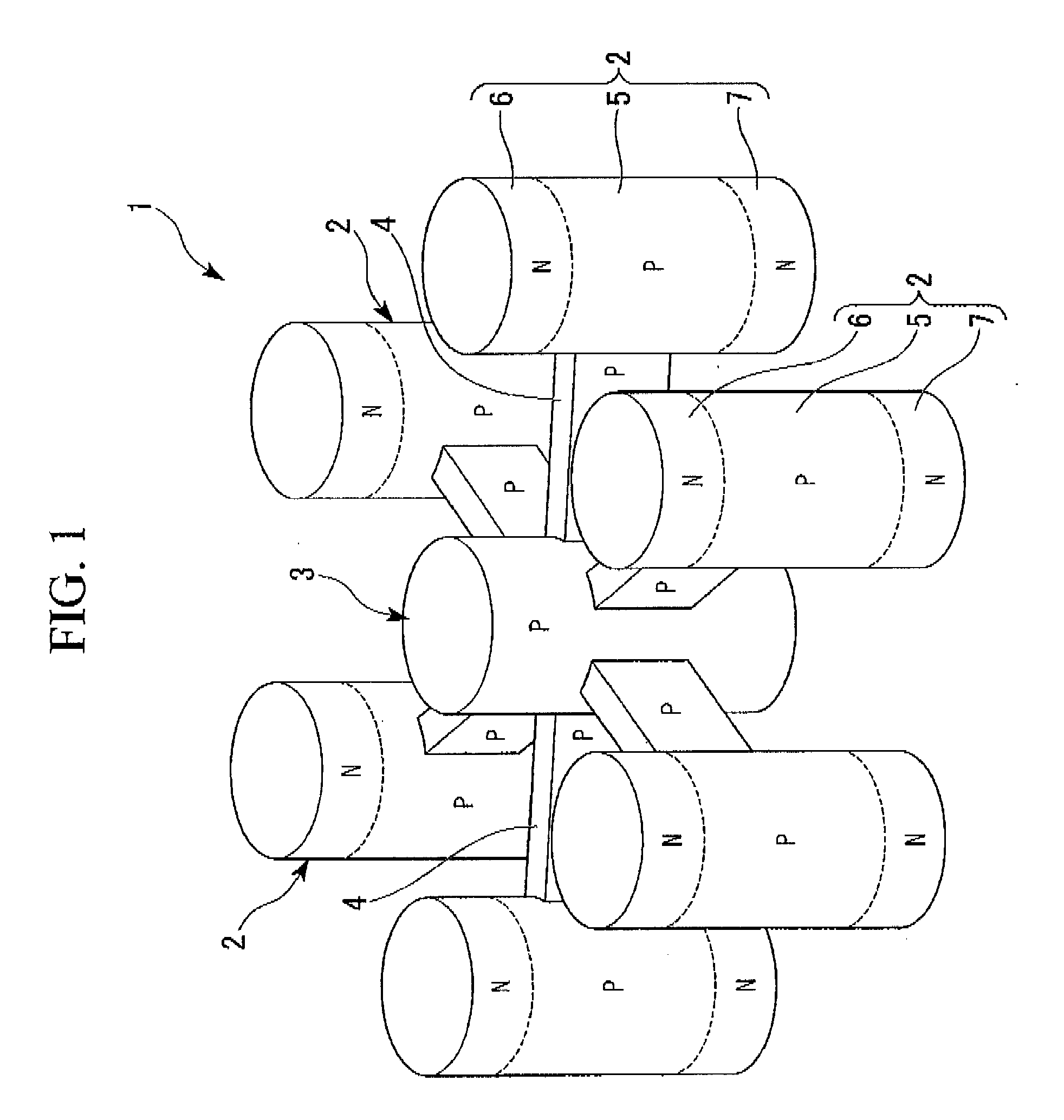
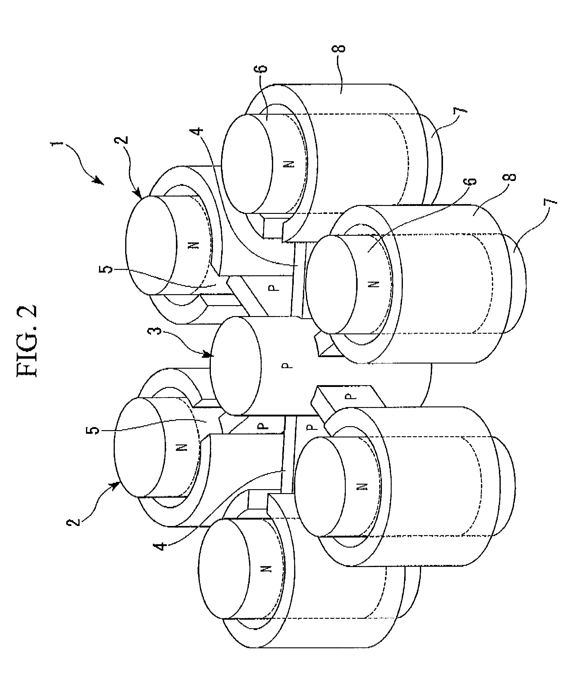
[0057]FIG. 1 shows a fundamental constitutional portion (silicon portion) of a three-dimensional transistor 1 which is an N-channel MOS (N-MOS) transistor. The fundamental constitutional portion is constituted from 7 pillars including one pillar which is at the center of the fundamental constitutional portion and which is surrounded by 6 other pins that are arranged so as to have equally-spaced intervals between each other. Six sets of the first pillars 2, not including the center portion of the fundamental constitutional portion, constitute six transistors. The second pillar 3 is arranged at the center portion of the fundamental constitutional portion and is connected to side walls of the channel portions 5 of six sets of the first pillars 2 via channel connection portions 4 which are P type.

[0058]The first pillar 2 has a center portion constituted from the channe...


PUM


Abstract

In order to provide a highly integrated semiconductor apparatus and a production method thereof which can avoid the floating of a channel portion that causes a problem when constituting a memory cell from three-dimensional transistors, a semiconductor apparatus includes: multiple three-dimensional transistors each of which includes: a first pillar; a channel portion provided at the first pillar; diffused layers formed at both an upper portion and a lower portion of the channel portion; and a gate electrode provided around the channel portion via a gate insulation film; and a second pillar which is electrically conductive, wherein the multiple three-dimensional transistors are arranged on a well area while surrounding the second pillar, the multiple three dimensional transistors share the second pillar, and the channel portions of the multiple three dimensional transistors are each connected to the second pillar by a channel connection portion. In addition, six three-dimensional transistors preferably share the second pillar which is a single pillar.

Description

BACKGROUND OF THE INVENTION[0001]1. Field of the Invention[0002]The present invention relates to a semiconductor apparatus which includes a three-dimensional transistor and a production method thereof.[0003]Priority is claimed on Japanese Patent Application No. 2007-150284, filed Jun. 6, 2007, the content of which is incorporated herein by reference.[0004]2. Description of the Related Art[0005]Because of requirements for a high integration in the semiconductor field, elements of the semiconductor apparatus have been being small and fine. Due to such requirements, a three-dimensional transistor has been developed in which elements are vertically arranged in order to integrate more elements in a smaller area compared to that of a conventional planer transistor.[0006]There is a generally-known constitution of such a three-dimensional transistor called SGT (surrounding gate transistor).[0007]In a constitution of SOT, for example, as shown in FIG. 13, a silicon pin 101 which constitutes ...

Claims


Application Information

Patent Timeline
IPC IPC(8): H01L29/78H01L21/336
CPCH01L21/743H01L27/11H01L27/1104H01L29/0657H01L29/66666H01L29/66787H01L29/7827H10B10/00H10B10/12
Inventor OYU, KIYONORI
Owner LONGITUDE LICENSING LTD
Why Eureka
Try Eureka