Back-illuminated type imaging device and fabrication method thereof

a technology of back illumination and imaging device, which is applied in the manufacture of semiconductor/solid-state devices, semiconductor devices, electrical devices, etc., can solve the problems of increasing fabrication cost, fixed pattern noise, and becoming more difficult to perform such a removal work, so as to prevent the increase of fabrication cost and the resistance between pads and wirings

Inactive Publication Date: 2008-12-18
FUJIFILM CORP
View PDF4 Cites 68 Cited by
  • Summary
  • Abstract
  • Description
  • Claims
  • Application Information

AI Technical Summary

Benefits of technology

[0011]The invention has been made in view of such circumstances, and provides a back-illuminated type imaging device that can prevent the fabrication cost and the resistance between pads and wirings from increasing even if pad openings is formed on a light incidence side.
[0035]According to the above configurations and methods, it is possible to provide a back-illuminated type imaging device capable of preventing the fabrication cost and the resistance between pads and wirings from increasing even if a pad opening is provided on a light incidence side.

Problems solved by technology

For this reason, if the pad opening is formed on the front-surface side of the semiconductor substrate in the back-illuminated type imaging device, it becomes necessary to drastically change or modify the test equipments, which may increase the fabrication cost.
However, such a method has the following problems.
That is, if the through hole is formed before the color filter or the microlens are formed on the back-surface side, a material for the color filter or the microlens may be left in the through hole and cannot be removed in subsequent steps.
Or, since the substrate on which the material is to be deposited has a large step formed thereon, the thickness of the deposited material is not even, which may cause a fixed pattern noise that appears as oblique lines in an image.
Moreover, even if the through hole is formed after the color filter or the microlens is formed, it is necessary to remove a photoresist that defines the through hole without causing any harm to the color filter or the microlens, which is very troublesome.
In particular, as described above, in the semiconductor substrate having a thickness of 10 μm, the above problems may become conspicuous, and it becomes more difficult to perform such a removal work.
Such a process step cannot be said to be practical as a semiconductor fabrication process.
However, in such a case, there arises a problem that the resistance of the conductive material filled in the trench may increase, which may affect the device characteristics.

Method used


Image

  • Back-illuminated type imaging device and fabrication method thereof
  • Back-illuminated type imaging device and fabrication method thereof
  • Back-illuminated type imaging device and fabrication method thereof

Examples


Embodiment Construction

[0044]Hereinafter, embodiments of the invention will be described with reference to the accompanying drawings.

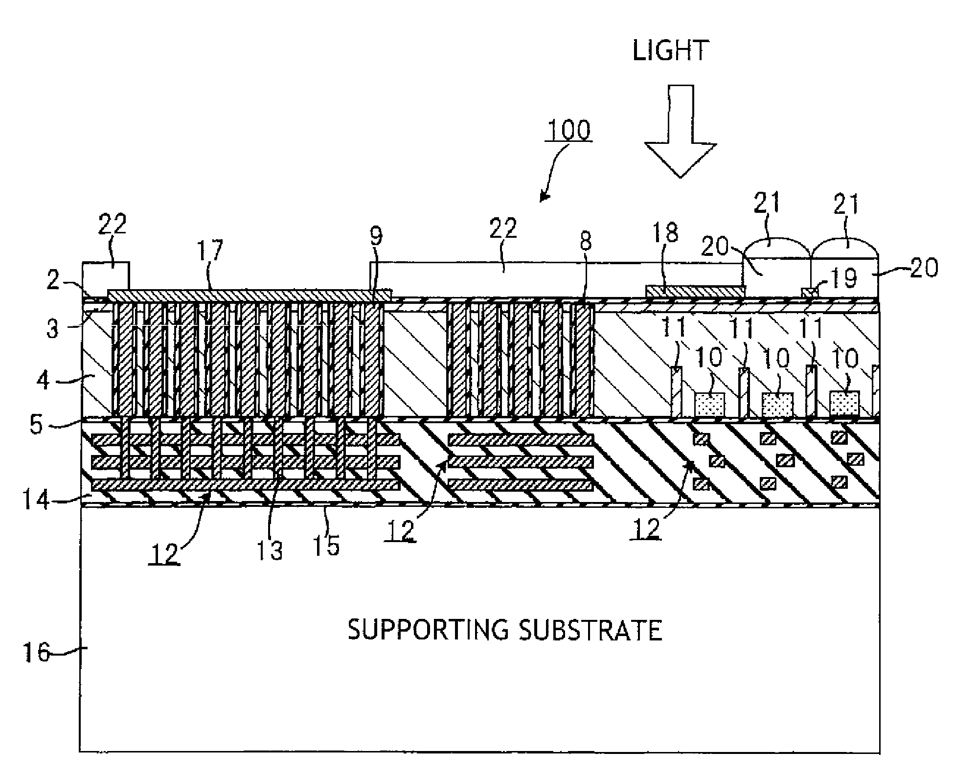
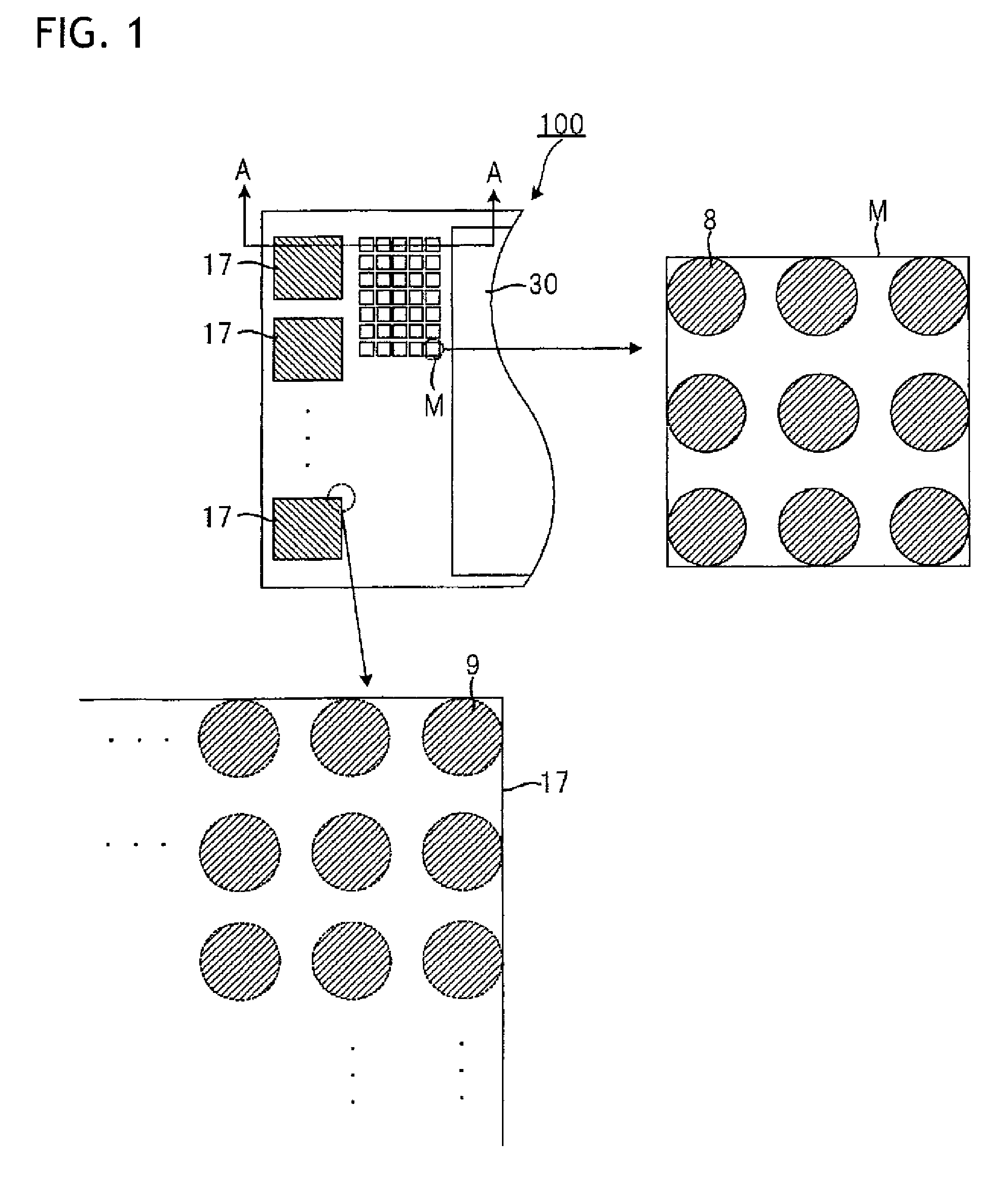
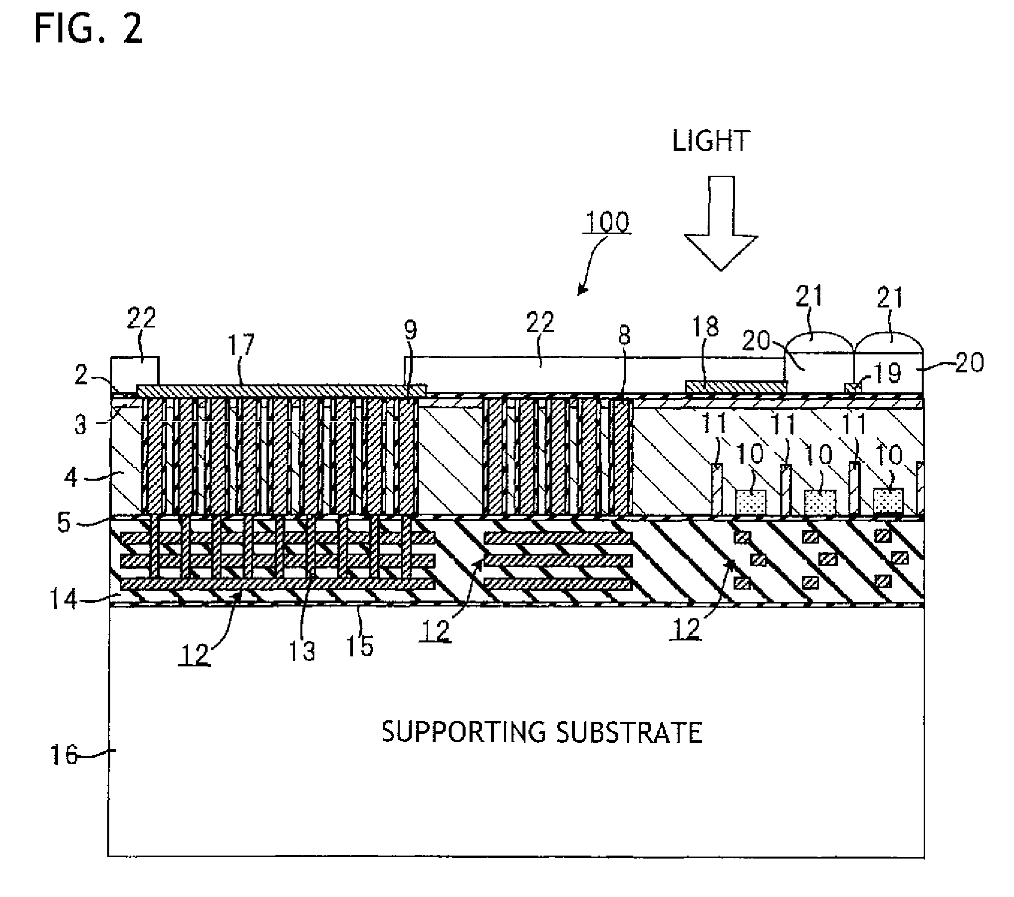
[0045]FIG. 1 is a schematic plan view of a back-illuminated type imaging device according to an embodiment of the invention, when viewed from a light incidence side (a back-surface side). FIG. 2 is a schematic sectional view taken along the line A-A of FIG. 1.

[0046]As shown in FIG. 1, the back-illuminated type imaging device 100 includes an imaging area 30 for receiving light to perform imaging; a mark forming area in which formed are a large number of alignment marks M that are used to align components (charge storage areas for storing charges, a signal output portion for outputting signals corresponding to the charges stored in the charge storage areas, and the like) on a front-surface side opposite to the back surface, in which the imaging area 30 is formed, with components on the back-surface side; and a pad forming area in which a large number of pad portions 17 that ar...


PUM


Abstract

Light is illuminated from a back-surface side of a silicon substrate 4. A back-illuminated type imaging device 100 reads out, from a front-surface side of the silicon substrate 4, charges that are generated in the silicon substrate 4 in response to the illuminated light, so as to perform imaging. The back-illuminated type imaging device 100 includes pad portions 17 formed on the back surface of the semiconductor substrate 4, and a plurality of pillars 9 that are formed in the semiconductor substrate 4, are made of a conductive material and electrically connect wiring portions 12 formed on the front surface of the semiconductor substrate 4 and the pad portions 17 to each other.

Description

CROSS-REFERENCE TO RELATED APPLICATIONS[0001]This application is based upon and claims the benefit of priority from the Japanese Patent Application No. 2007-157460 filed on Jun. 14, 2007, the entire contents of which are incorporated herein by reference.BACKGROUND OF THE INVENTION[0002]1. Technical Field[0003]The invention relates to a back-illuminated type imaging device in which light is illuminated from a back-surface side of a semiconductor substrate and charges that are generated in the semiconductor substrate in response to the light are read from a front-surface side of the semiconductor substrate to perform imaging.[0004]2. Description of the Related Art[0005]The following back-illuminated type imaging device has been proposed. That is, light is illuminated from a back-surface side of a semiconductor substrate. The back-illuminated type imaging device stores charges that are generated in the semiconductor substrate in response to the light, into charge storage areas formed o...

Claims


Application Information

Patent Timeline
Patent Type & Authority Applications(United States)
IPC IPC(8): H01L31/0216H01L31/18
CPCH01L27/14603H01L27/1464H01L27/14636
Inventor UYA, SHINJI
Owner FUJIFILM CORP
Why Eureka
Try Eureka