Substrate for manufacturing semiconductor device and manufacturing method thereof

Inactive Publication Date: 2008-12-18
SEMICON ENERGY LAB CO LTD
View PDF25 Cites 32 Cited by
  • Summary
  • Abstract
  • Description
  • Claims
  • Application Information

AI Technical Summary

Benefits of technology

[0010]In view of the above problem, it is an object of the present invention to provide a substrate for manufacturing a semiconductor device with improved electric characteristics, and a manufacturing method thereof. Further, it is another object to provide a semiconductor device with high reliability and a manufacturing method thereof.
[0024]Employment of a substrate for manufacturing a semiconductor device according to the present invention can improve electric characteristics in manufacturing a semiconductor device. Further, manufacture of a semiconductor device with improved reliability can be realized.

Problems solved by technology

In a case of forming a single-crystalline semiconductor film on a different kind of substrate from a semiconductor substrate, a problem can be caused due to impurities in the different kind of substrate.
For example, in an SOI substrate in which a single-crystalline semiconductor film is formed on a glass substrate, metal impurities such as an alkali metal or an alkaline earth metal in the glass substrate are diffused into the single-crystalline semiconductor film through heat treatment, unfortunately.
In a case of manufacturing a field-effect transistor using the single-crystalline semiconductor film, diffusion of metal impurities leads to characteristic degradation, and causes reduction in reliability.

Method used


Image

  • Substrate for manufacturing semiconductor device and manufacturing method thereof
  • Substrate for manufacturing semiconductor device and manufacturing method thereof
  • Substrate for manufacturing semiconductor device and manufacturing method thereof

Examples


embodiment modes

[0042]Hereinafter, embodiment modes of the present invention are described with reference to the drawings. Note that the present invention is not limited to the following description, and it is easily understood by those skilled in the art that the modes and details disclosed herein can be modified in various ways without departing from the spirit and scope of the present invention. Therefore, the present invention should not be interpreted as being limited to the description of the embodiment modes to be given below. In the structures of the present invention to be described hereinafter, a reference numeral which designates the same parts is used in different drawings in some cases.

embodiment mode 1

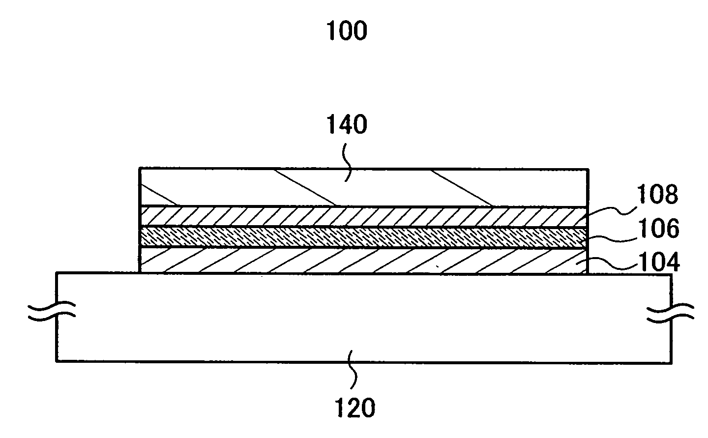
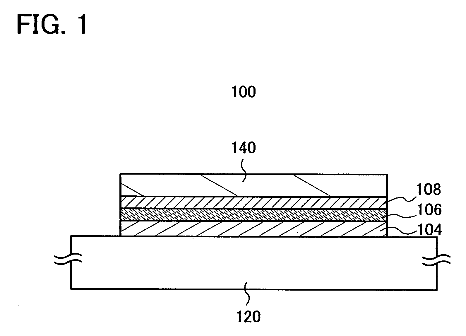
[0043]A substrate for manufacturing a semiconductor device of this embodiment mode has an SOI structure, and is formed by transferring a semiconductor film separated from a semiconductor substrate, preferably a single-crystalline semiconductor film separated from a single-crystalline semiconductor substrate, to a supporting substrate. As the supporting substrate, a substrate whose main component is different from that of the semiconductor substrate is used. FIG. 1 shows a mode of a substrate for manufacturing a semiconductor device of this embodiment mode.

[0044]In a substrate 100 for manufacturing a semiconductor device in FIG. 1, a stacked-layer structure of a first silicon oxide film 104, a silicon nitride film 106, and a second silicon oxide film 108 is formed on a supporting substrate 120, and a semiconductor film 140 is formed on the stacked-layer structure. The semiconductor film 140 is fixed over the supporting substrate 120 with the first silicon oxide film 104, the silicon ...

embodiment mode 2

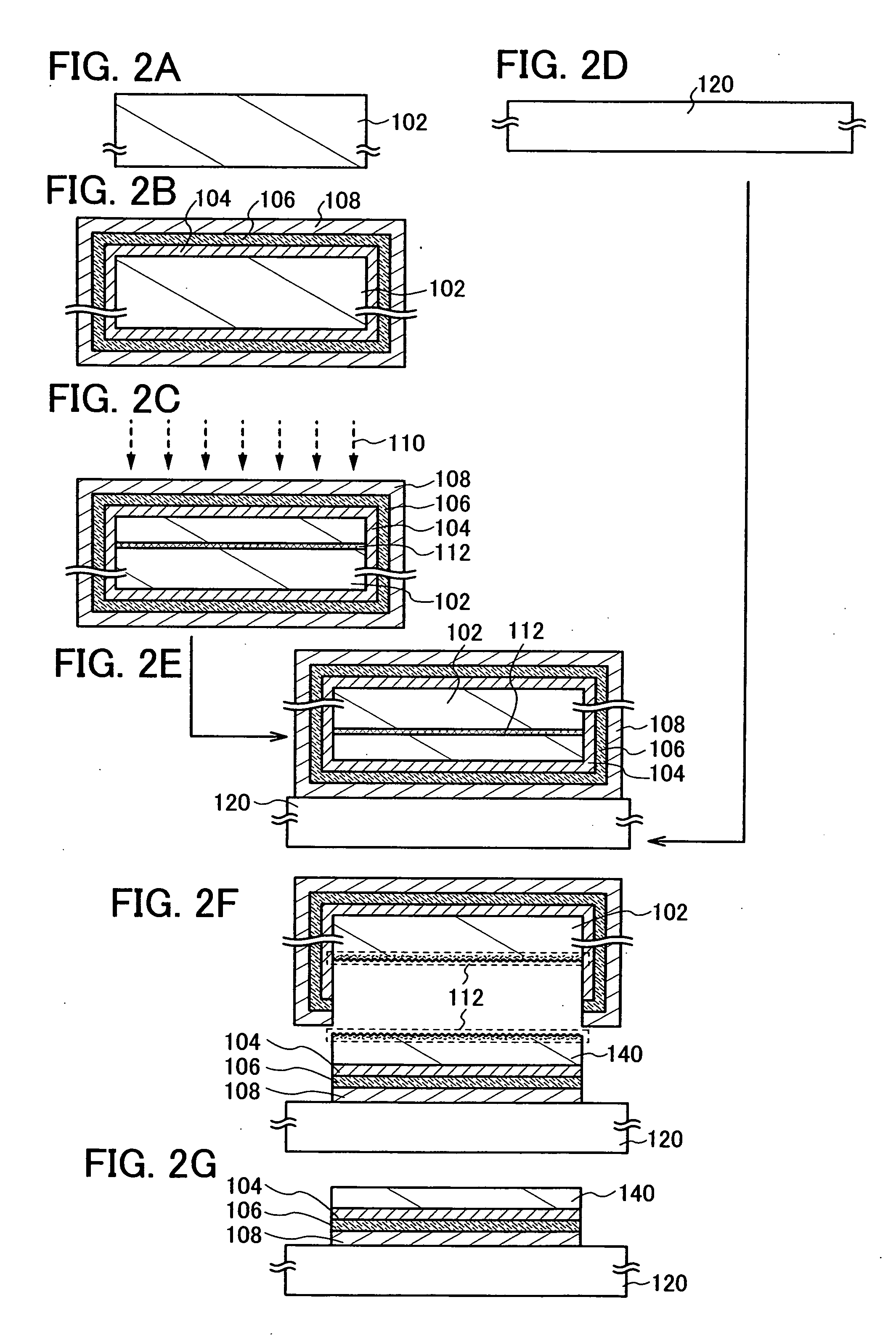
[0120]This embodiment mode illustrates an example in which a semiconductor device is manufactured using a substrate for manufacturing a semiconductor device according to the present invention, with reference to FIGS. 6A to 7B.

[0121]A substrate for manufacturing a semiconductor device is prepared (see FIG. 6A). This mode shows an example in which a substrate for manufacturing a semiconductor device with an SOI structure in which the semiconductor film 140 is fixed over the supporting substrate 120 with the stacked second silicon oxide film 108, the silicon nitride film 106, and the first silicon oxide film 104 interposed therebetween as shown in FIG. 1 is used. The present invention does not have any particular limitation, and a substrate for manufacturing a semiconductor device with another structure shown in this specification can be employed.

[0122]The semiconductor film 140 has a thickness of 5 to 500 nm inclusive, preferably 10 to 200 nm inclusive, more preferably 10 to 60 nm inc...


PUM


Abstract

A substrate with which a semiconductor device with excellent electric characteristics and high reliability can be manufactured is provided. An aspect of the invention is a method for manufacturing a substrate for manufacturing a semiconductor device: a first silicon oxide film, a silicon nitride film, and a second silicon oxide film are stacked in this order over a surface of a semiconductor substrate by a thermal CVD method, and then a weakened layer is formed at a given depth of the semiconductor substrate; the semiconductor substrate and a substrate having an insulating surface are arranged to face each other, and the second silicon oxide film provided for the semiconductor substrate and a supporting substrate are bonded to each other; and the semiconductor substrate is separated at the weakened layer by heat treatment, whereby a semiconductor film separated from the semiconductor substrate is left over the substrate having the insulating surface.

Description

BACKGROUND OF THE INVENTION[0001]1. Field of the Invention[0002]The present invention relates to a substrate for manufacturing a semiconductor device with an SOI (silicon on insulator) structure and to a manufacturing method thereof.[0003]In this specification, a semiconductor device means a device in general which can operate utilizing semiconductor characteristics. An electrooptic device, a semiconductor circuit, and an electronic device are all included in the category of the semiconductor device.[0004]2. Description of the Related Art[0005]With development in VLSI technology, demanded levels of integration, operation speed, and power consumption have been higher. In order to satisfy these requirements, an SOI structure is receiving attention. In this technology, an active region (channel formation region) of a field-effect transistor (FET), which is conventionally formed with bulk single-crystalline silicon, is formed with a single-crystalline silicon thin film. It is known that...

Claims


Application Information

Patent Timeline
IPC IPC(8): H01L21/86H01L27/12
CPCH01L21/76254H01L27/1214H01L27/1266H01L29/66772H01L2924/0002H01L2924/00H01L27/12
Inventor KAKEHATA, TETSUYAKURIKI, KAZUTAKA
Owner SEMICON ENERGY LAB CO LTD
Why Eureka
Try Eureka