Electronic Circuit and Semiconductor Device Having Dac and Scf

a technology of electronic circuit and semiconductor device, which is applied in the direction of digital-analog converters, transmission systems, instruments, etc., can solve the problems of increasing the clock feed-through of the transistor, affecting the operation of the transistor, and causing the output of the scf to be affected, so as to facilitate the reduction of clock feed-through, reduce the resistance of the switch, and reduce the error of the circuit

Inactive Publication Date: 2008-12-25
ROHM CO LTD
View PDF1 Cites 4 Cited by
  • Summary
  • Abstract
  • Description
  • Claims
  • Application Information

AI Technical Summary

Benefits of technology

[0026]The inventive electronic circuit may include a voltage selection output circuit in the form of a DAC, for example, and other circuits such as an SCF in which operational conditions of the input side switch of the SCF are incorporated in the selection conditions for selecting respective multiple selection switches of the voltage selection and output circuit. Thus, dedicated input side switch of the SCF can be omitted to reduce the number of series switches such as MOS transistors.
[0027]Hence, on-resi

Problems solved by technology

However, the buffer amplifier 13 not only incurs errors in the output of the SCF 20 due to the non-linearity of the buffer amplifier itself, but also consumes extrapower for its operation (that is proportional to the current through it).
However, if the on-resistance of each MOS transistor is reduced

Method used


Image

  • Electronic Circuit and Semiconductor Device Having Dac and Scf
  • Electronic Circuit and Semiconductor Device Having Dac and Scf
  • Electronic Circuit and Semiconductor Device Having Dac and Scf

Examples


Embodiment Construction

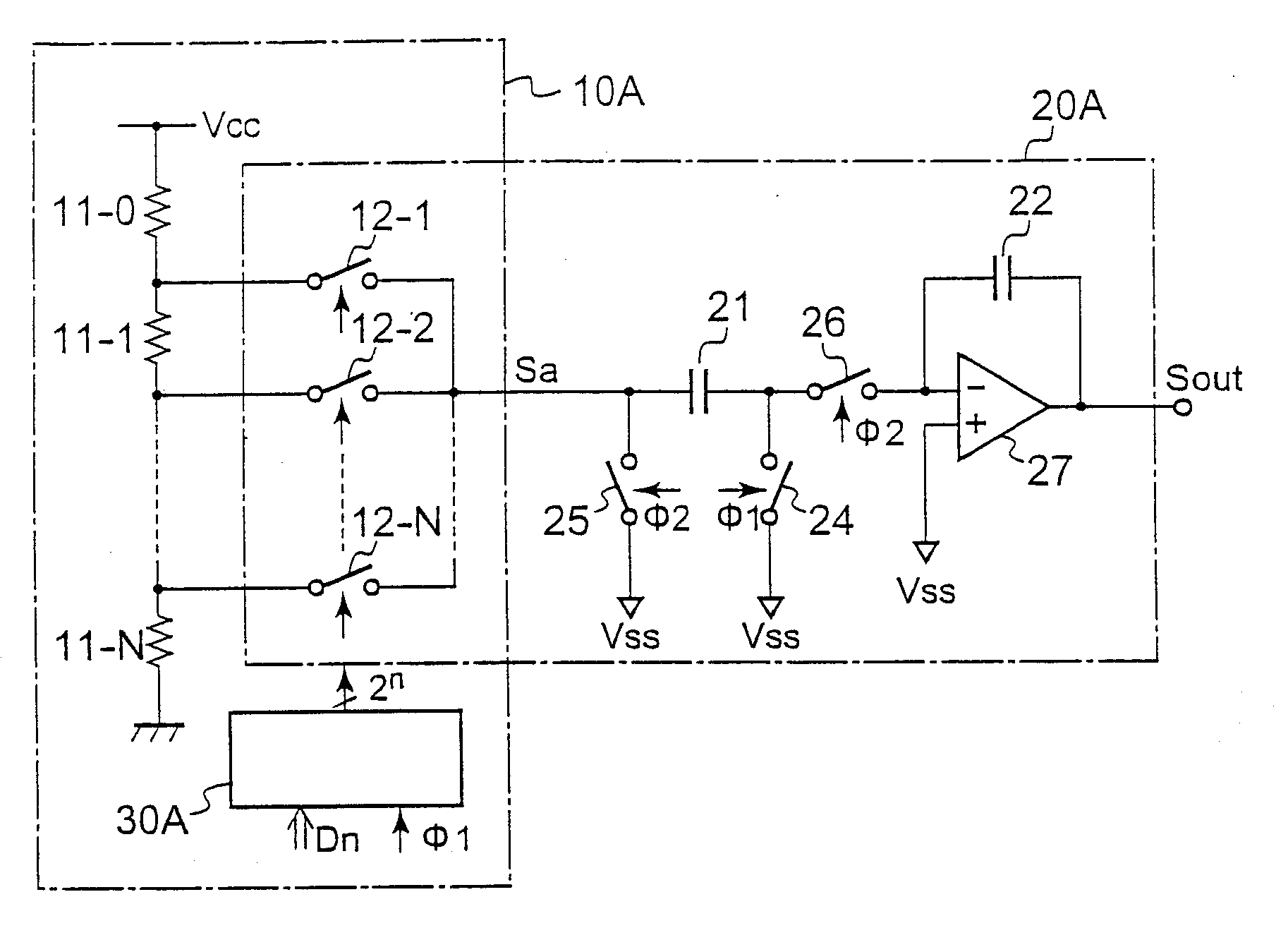
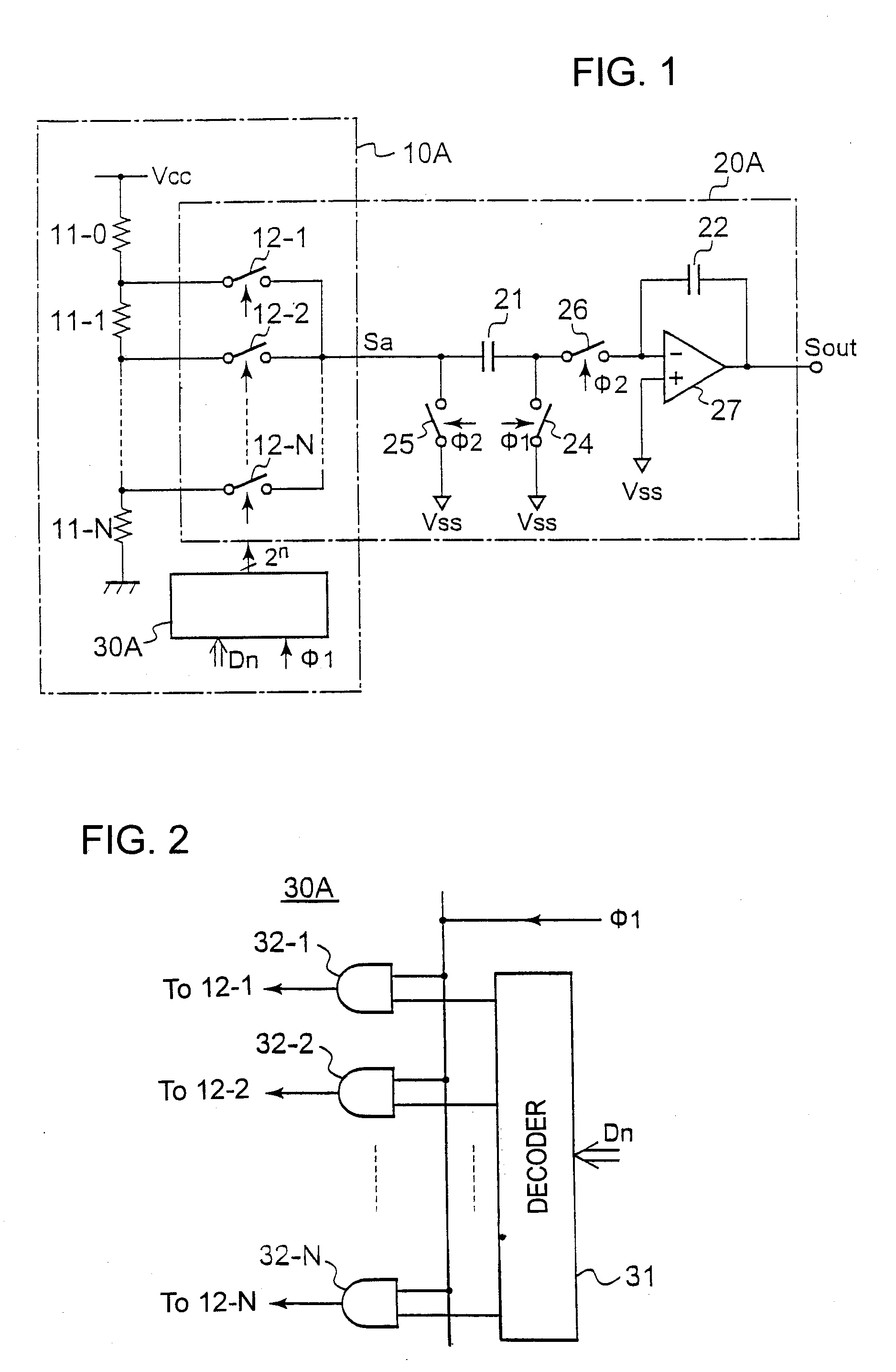
[0035]An inventive electronic circuit will now be described in detail with reference to the accompanying drawings. Incidentally, since the electronic circuit of the invention is built in an LSI, it can be referred to as a semiconductor device.

[0036]Referring to FIG. 1, there is shown the arrangement of an electronic circuit in accordance with a first embodiment of the invention.

[0037]As shown in FIG. 1, the electronic circuit is provided with a DAC 10A for converting an inputted digital signal Dn into an analog signal (analog voltage) Sa, and an SCF 20A for filtering the analog signal Sa outputted from the DAC 10A. The DAC 10A and SCF 20A may be used in various electric devices for processing signals. The DAC 10A can be any voltage selection output circuit capable of selecting voltages from multiple different voltages one at a time by means of multiple selection switches, and outputting the voltage thus selected.

[0038]It is seen that the conventional buffer amplifier 13 as shown in ...


PUM


Abstract

An electronic circuit has a voltage selection and output circuit, e.g. digital-to-analog converter (DAC), and a switched capacitor filter (SCF), in which operational conditions of the input side switches of the SCF are incorporated in the selection conditions for selecting respective multiple selection switches of the voltage selection and output circuit. This arrangement permits the selection switches to serve as the input side switches, thereby reducing in number serial switches such as MOS transistors in the circuit, and hence reducing the on-resistances of the serial switches, while preventing the clock feed-through thereof from increasing and suppressing output errors due to the linearity error of the buffer amplifier involved.

Description

BACKGROUND OF THE INVENTION[0001]1. Field of the Invention[0002]This invention relates to an electronic circuit and a semiconductor device, equipped with a digital-to-analog converter (DAC) and a switched capacitor filter circuit (SCF).[0003]2. Description of the Related Art[0004]Conventionally, a DAC for converting a digital signal into an analog signal and a SCF for filtering the analog signal outputted from the DAC are used in signal processing circuits of various electronic apparatuses (see, for example, Japanese Patent Applications Laid Open H11-308108 and H06-204866).[0005]A typical DAC 10 and an SCF 20 have arrangements as shown in FIG. 6. The DAC 10 of FIG. 6 includes a resistive voltage division circuit having series resistors 11-0-11-N connected between a power supply voltage Vcc and the ground. Connected to each node of the serially connected voltage division resistors 11-0-11-N is each one end of associated selection switches 12-1-12-N. Opposite ends of these selection s...

Claims


Application Information

Patent Timeline
IPC IPC(8): H03M1/66H03M3/02
CPCH03M1/0818H03M1/765H03M3/368H03M3/454
Inventor CHIDA, TAISUKE
Owner ROHM CO LTD
Why Eureka
Try Eureka