

Optical waveguide device
a technology of optical waveguides and light guides, applied in the field of optical waveguide devices, can solve problems such as the difficulty of solving the subject described above, and achieve the effect of improving the modulation efficiency of driving voltag
- Summary
- Abstract
- Description
- Claims
- Application Information
AI Technical Summary
Benefits of technology
Problems solved by technology
Method used
Image

Examples
first embodiment
[A] Description of the First Embodiment
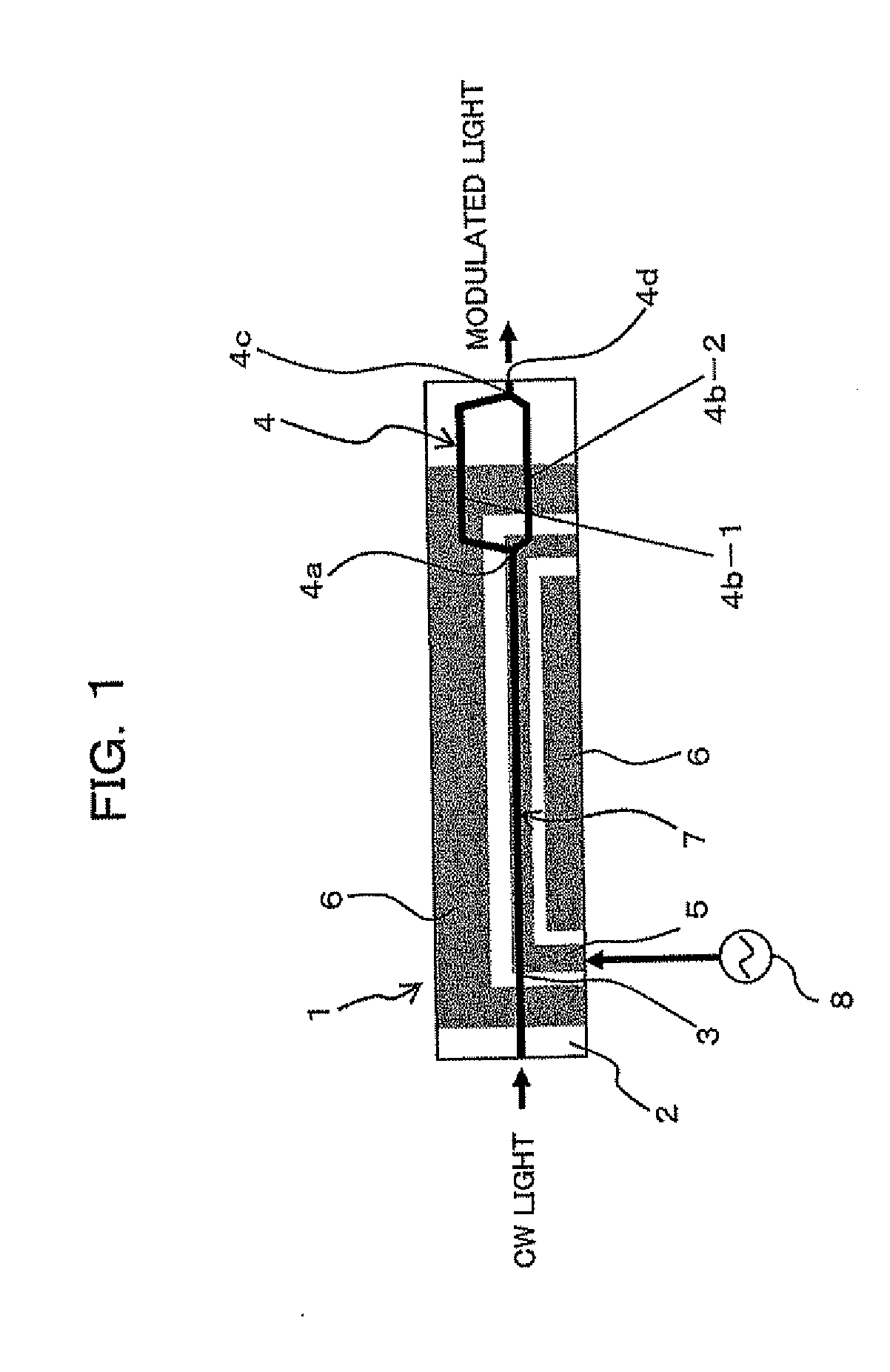
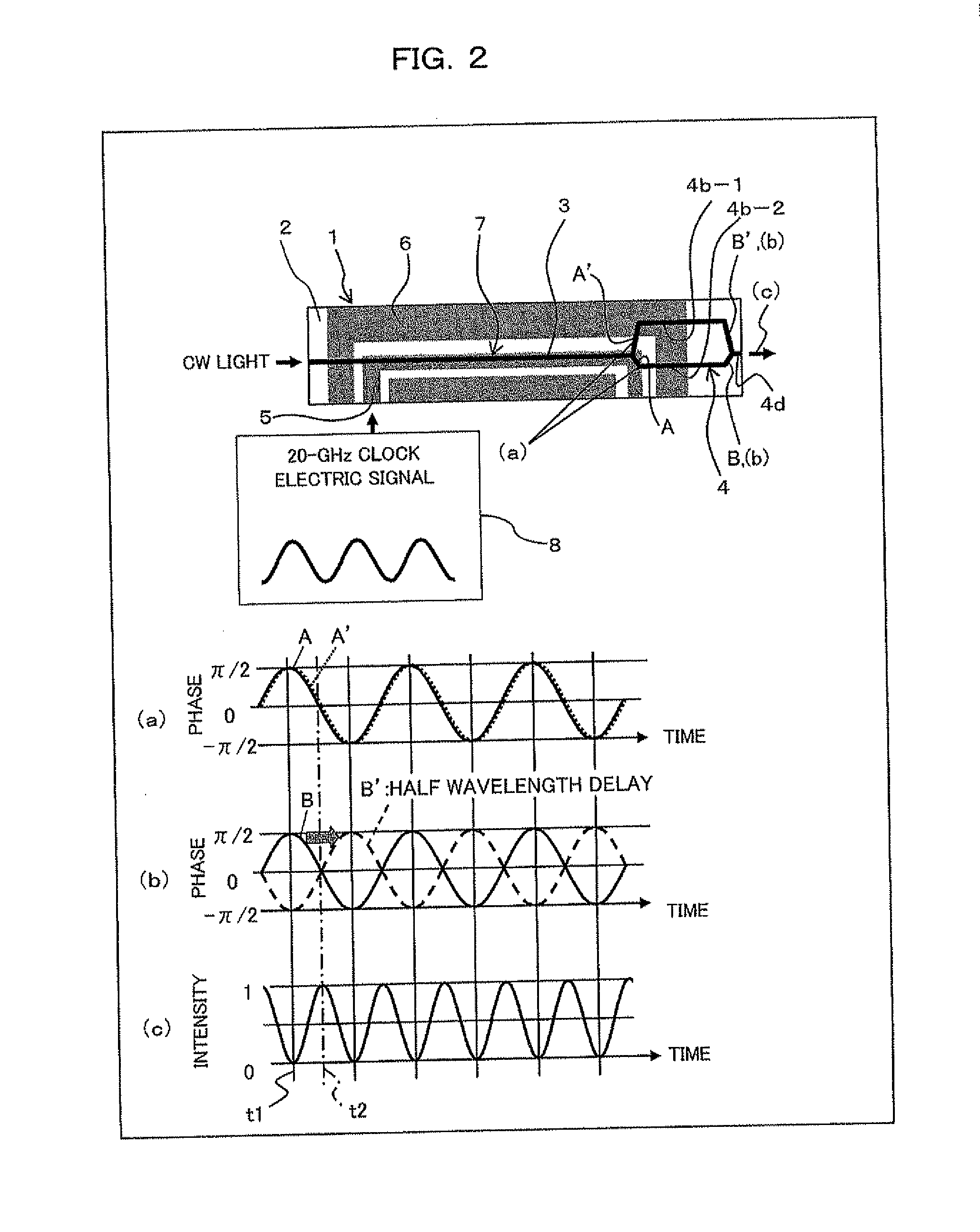
[0043]FIG. 1 is a schematic top plan view showing an optical waveguide device 1 according to a first embodiment of the present invention. Referring to FIG. 1, the optical waveguide device 1 shown includes a substrate 2 having an electro-optical effect such as Z-cut LN, and an optical waveguide 3 and a Mach-Zehnder interferometer 4 formed on the substrate 2 and connected to the optical waveguide 3. Similarly as in the case of FIG. 12, the optical waveguide 3 and the Mach-Zehnder interferometer 4 are formed on the substrate 2 by Ti diffusion or proton exchange.
[0044]Further, a phase modulation electrode 5 for supplying a clock signal is formed on the optical waveguide 3. It is to be noted that ground electrodes 6 are formed in a predetermined spaced relationship around the phase modulation electrode 5. Further, an electric signal having, for example, a frequency of 20 GHz is supplied as a clock signal from a clock signal source 8 to the phase mod...
second embodiment
[B] Description of the Second Embodiment
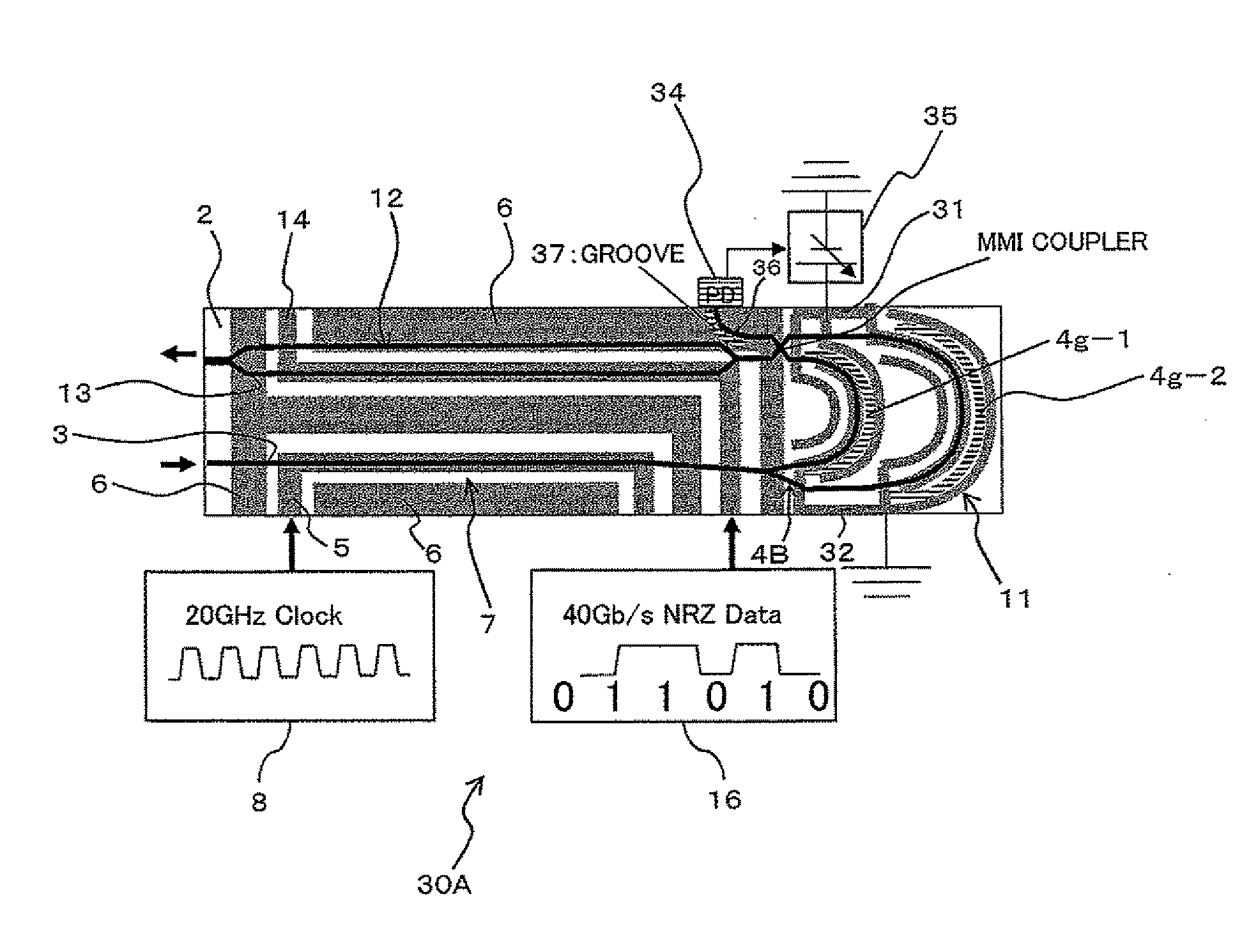
[0062]FIG. 5 is a schematic top plan view showing an optical waveguide device 10 according to a second embodiment of the present invention. In the optical waveguide device 10 shown in FIG. 5, a clock modulation section 11 is provided as a configuration which forms the optical waveguide device 1 according to the first embodiment described above, and a configuration as a data modulation section 12 is integrally formed on the same substrate 2. It is to be noted that, in FIG. 5, like elements to those in FIG. 1 are denoted by like reference characters.
[0063]In particular, as the clock modulation section 11, an optical waveguide 3, a phase modulation electrode 5 and ground electrodes 6 which form a phase modulation section 7 are provided on the substrate 2, and a Mach-Zehnder interferometer 4 connected to the optical waveguide 3 is formed on the downstream side in a light propagation direction with respect to the optical waveguide 3.
[0064]The data ...
third embodiment
[C] Description of the Third Embodiment
[0069]FIG. 6 is a schematic top plan view showing an optical waveguide device 20 according to a third embodiment of the present invention. While, also with the optical waveguide device 20 shown in FIG. 6, reduction of the device size can be implemented through a region of curved and folded back waveguides, particularly the curved and folded back waveguide region is provided on a Mach-Zehnder interferometer 4B. It is to be noted that, in FIG. 6, like elements to those in FIG. 5 are denoted by substantially like reference characters.
[0070]In particular, as seen in FIG. 6, the Mach-Zehnder interferometer 4B includes two branching waveguides 4f-1 and 4f-2 curved and folded back in a semi-circular shape and having lengths different from each other, a branching portion 4a for branching light propagated through the optical waveguide 3 which forms the phase modulation section 7 into two lights and connecting the two lights to the branching waveguides 4...
PUM
| Property | Measurement | Unit |
|---|---|---|
| frequency | aaaaa | aaaaa |
| thickness | aaaaa | aaaaa |
| voltage amplitude | aaaaa | aaaaa |
Abstract
Description
Claims
Application Information