Recoverable electronic component

a technology of electronic components and components, applied in the direction of sustainable manufacturing/processing, final product manufacturing, synthetic resin layered products, etc., can solve the problems of low temperature thermoplastics that cannot be exposed to later processing steps such as curing, and cannot be remelted,

Inactive Publication Date: 2008-12-25
GENERAL ELECTRIC CO
View PDF63 Cites 21 Cited by
  • Summary
  • Abstract
  • Description
  • Claims
  • Application Information

AI Technical Summary

Problems solved by technology

In applications where the coefficient of thermal expansion (CTE) of the electronic device is not a close match for the CTE of the substrate upon which it is attached, thermal cycling will stress the solder joints and may cause solder fatigue failure.
Furthermore, low temperature thermoplastics cannot be exposed to later processing steps such as curing, or to certain assembly steps that exceed their melt or softening temperature.
The problem with the use of a thermoset underfill resin is that a thermoset cannot be remelted at a normal processing temperature; thus, the defective electronic device is not removable and the entire circuit must be discarded.
Accordingly, the use of low processing temperature, low stress thermoset adhesives results in a non-repairable processing step.
Furthermore, the remeltable, reworkable thermoplastic resins require high temperature processing, and result in high stress structures that are not compatible with many planned applications.
Additionally, in embedded chip applications in which an interconnect structure is directly attached to the surface of electronic components a similar issue arises.
In these applications, the use of a thermoplastic adhesive to bond the electronic component to the interconnect structure either stresses the structure excessively because of the high thermoplastic melt temperature or severely limits the components operating and / or assembly temperature because of a low thermoplastic melt temperature.
Use of a thermoset adhesive in these applications reduces the stress and increases the operating and assembly temperature range, but makes recovery of the electronic component extremely difficult if not impossible.
Since all complex interconnect structures have processing defects such as electrical shorts and / or opens, they also have inherent yield losses.
In the ECBU process, the chip is bonded to the interconnect structure prior to the fabrication of the interconnect structure, potentially causing a good chip to be scrapped with a bad package.

Method used


Image

  • Recoverable electronic component
  • Recoverable electronic component
  • Recoverable electronic component

Examples


Embodiment Construction

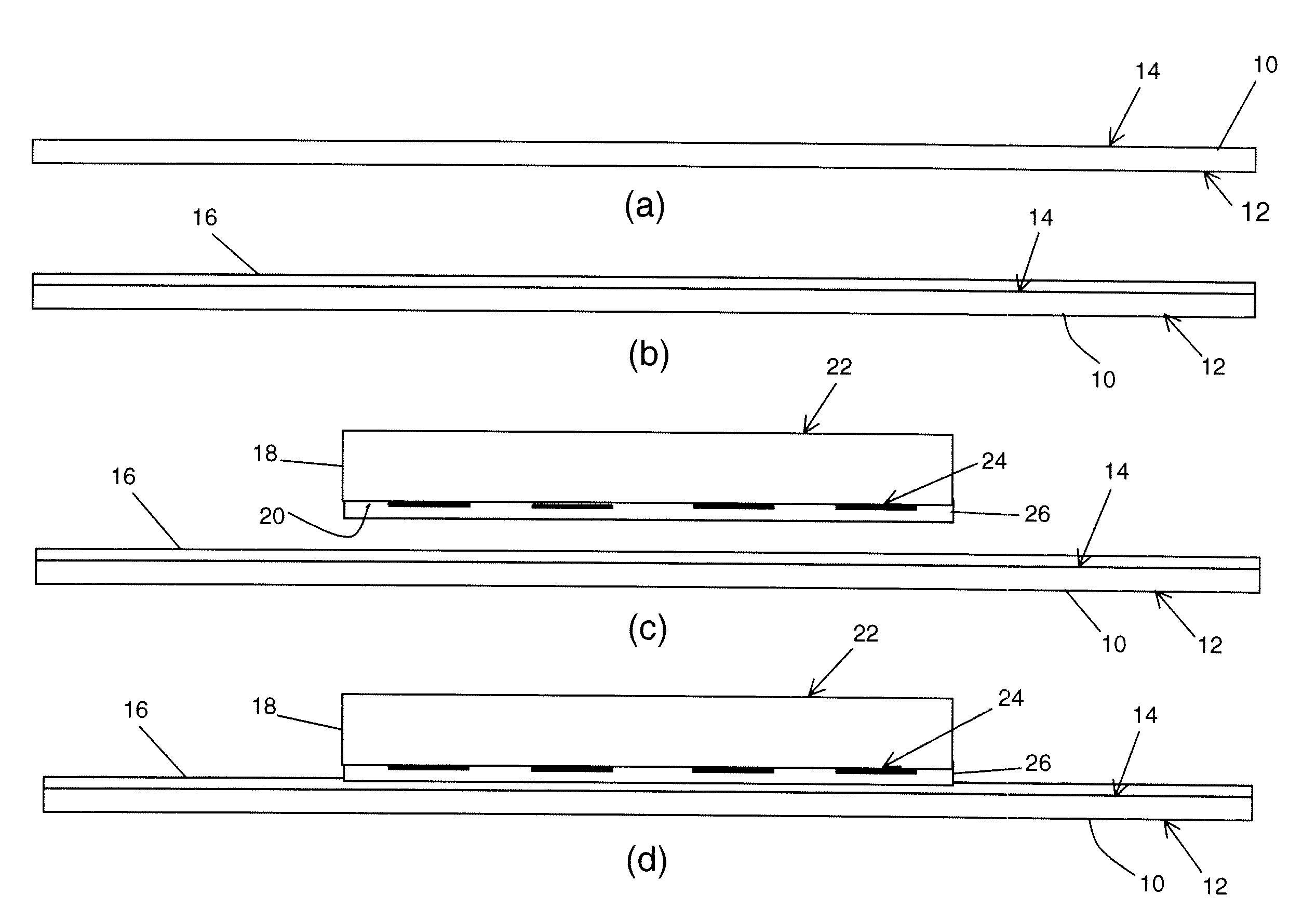
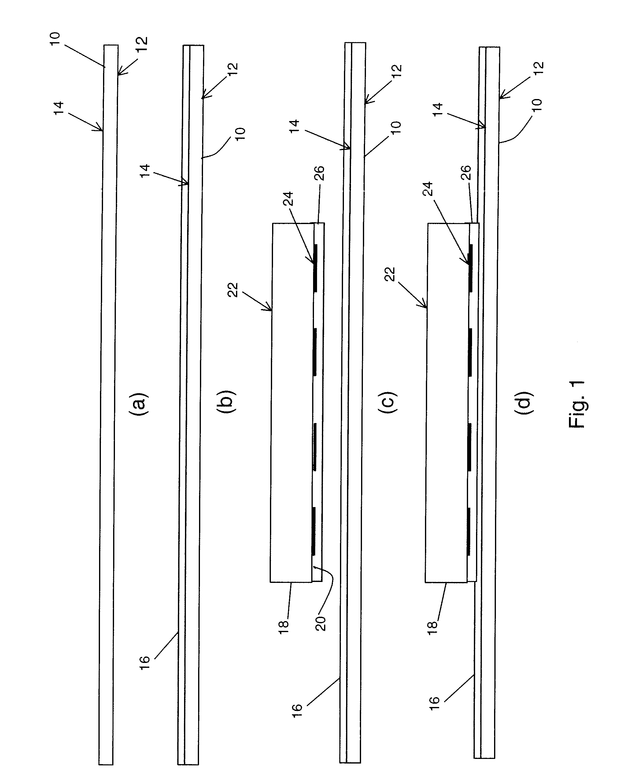
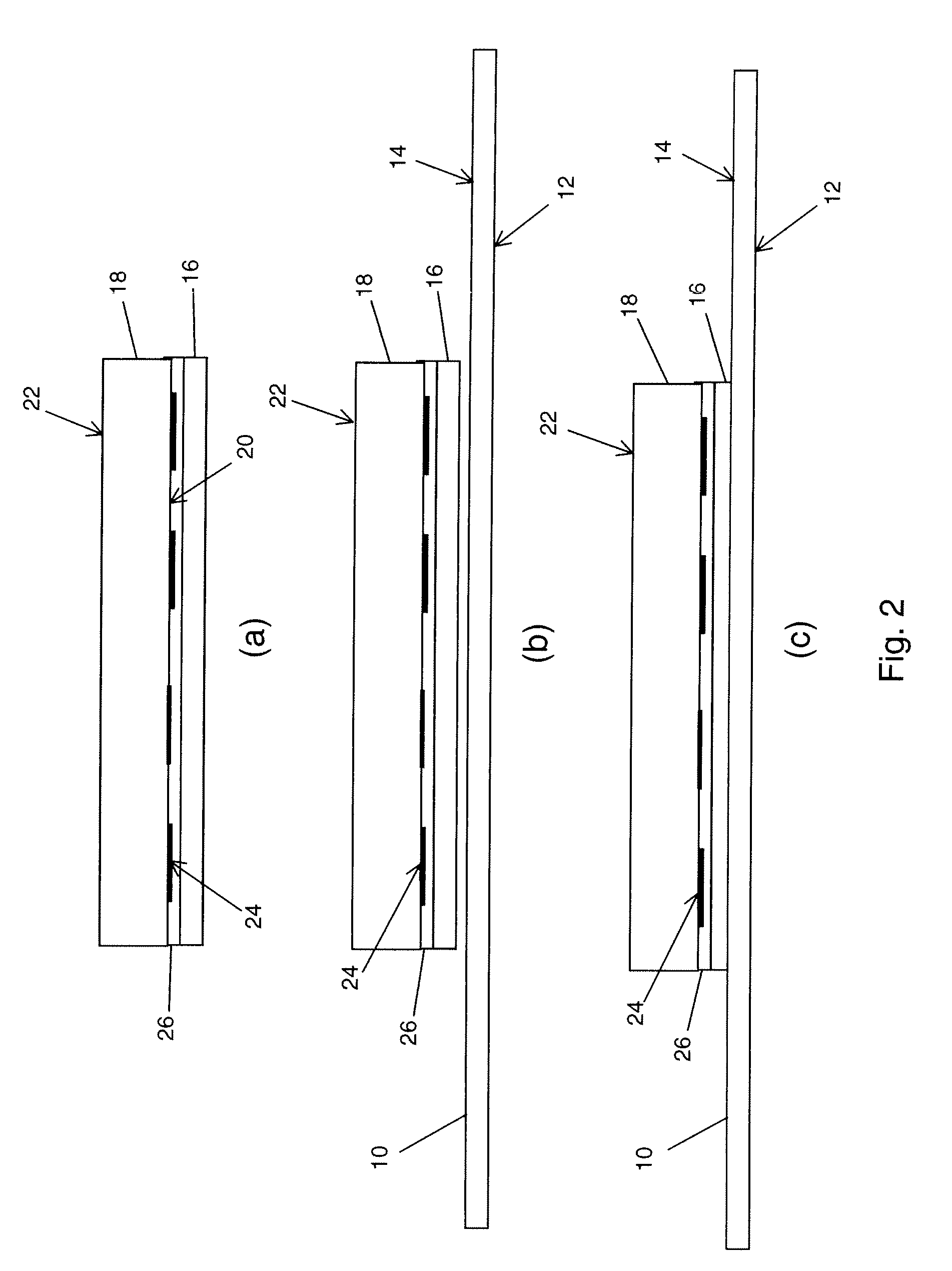
[0027]The invention includes embodiments that relate to the fabrication of an electronic device or interconnect structure. The invention embodiments that relate to a method of recovering a chip or other electrical component from the device. A method may provide for the recovery of an undamaged electronic device, such as a chip, from a defective interconnect structure or package. The methods may be useful in processes involving resin underfills and other embedded chip technology. However, the methods may be used in applications in which the recovery of an electronic device from an interconnect structure or package is desired.

[0028]The invention includes embodiments that relate to the fabrication of an electronic device or interconnect structure. The invention embodiments that relate to a method of recovering a chip or other electrical component from the device. A method may provide for the recovery of an undamaged electronic device, such as a chip, from a defective interconnect struc...


PUM

PropertyMeasurementUnit
thicknessaaaaaaaaaa
thicknessaaaaaaaaaa
temperatureaaaaaaaaaa

Abstract

An electronic component includes a base insulative layer having a first surface and a second surface; an electronic device having a first surface and a second surface, and the electronic device being secured to the base insulative layer; an adhesive layer disposed between the first surface of the electronic device and the second surface of the base insulative layer; and a removable layer disposed between the first surface of the electronic device and the second surface of the base insulative layer. The base insulative layer secures to the electronic device through the removable layer. The removable layer is capable of releasing the base insulative layer from the electronic device. The removal may be done without damage to a predetermined part of the electronic component.

Description

BACKGROUND[0001]1. Technical Field[0002]The invention includes embodiments that relate to the fabrication of an interconnect structure. The invention embodiments that relate to a method of recovering a chip or other electrical component from an interconnect structure.[0003]2. Discussion of Art[0004]Bonding of electronic devices such as semiconductor chips, discrete passives, BGA carriers or other electrical elements onto printed circuit boards, substrates, interconnect structures or flex circuits is generally done with solders or adhesives. In an area array solder attach assembly, the electrical connections are made by raising the temperature to reflow the solder, which solidifies upon cooling. In applications where the coefficient of thermal expansion (CTE) of the electronic device is not a close match for the CTE of the substrate upon which it is attached, thermal cycling will stress the solder joints and may cause solder fatigue failure. One method to overcome this issue is to en...

Claims


Application Information

Patent Timeline
Patent Type & Authority Applications(United States)
IPC IPC(8): B32B27/36B32B9/04H01L23/58
CPCH01L23/3128H01L23/36H01L23/5389H01L24/19H01L24/20H01L2224/04105H01L2224/12105H01L2224/131H01L2224/20H01L2224/221H01L2224/73267H01L2224/76155H01L2224/92144H01L2924/01005H01L2924/01013H01L2924/01015H01L2924/01027H01L2924/01029H01L2924/01051H01L2924/01073H01L2924/01074H01L2924/01078H01L2924/01079H01L2924/01082H01L2924/01322H01L2924/09701H01L2924/14H01L2924/1433H01L2924/15153H01L2924/1517H01L2924/15311H01L2224/24227H01L2924/014H01L2924/01006H01L2924/01019H01L2924/01024H01L2924/01033H01L2924/01047H05K1/185H05K1/0203H05K3/305H05K3/4644H05K2201/1056H05K2201/10674H05K2201/10984H05K2201/2018H05K2203/1469H05K2203/176H01L2924/10253H01L2924/00H01L2224/82102H01L2224/32245H01L2224/0401Y10T428/31507Y02P70/613H01L2224/83132H01L2224/32225H01L2224/83191Y02P70/50
Inventor FILLION, RAYMOND ALBERTESLER, DAVID RICHARDERLBAUM, JEFFREY SCOTTMILLS, RYAN CHRISTOPHERWOYCHIK, CHARLES GERARD
Owner GENERAL ELECTRIC CO
Why Eureka
Try Eureka