Method for Building MOS Transistor Model and Method for Verifying MOS Transistor Model

a transistor model and mos technology, applied in the field of building mos transistor models and mos transistor model verification methods, can solve the problems of deteriorating signal-to-noise rate, different dies and different runs, and devices in a circuit may typically give rise to various noises

Active Publication Date: 2008-12-25
SEMICON MFG INT (SHANGHAI) CORP
View PDF1 Cites 9 Cited by
  • Summary
  • Abstract
  • Description
  • Claims
  • Application Information

AI Technical Summary

Benefits of technology

[0004]The present invention addresses a problem in the prior art that a conventional MOS transist...

Problems solved by technology

Currently, devices in a circuit may typically give rise to various noises.
The 1/f noise primarily influences devices operating in a low frequency environment.
However in some radio frequency circuits, such as frequency mixer, amplifier and frequency divider, etc., the 1/f noise has an increasing influence in high frequency band, and may result in a deteriorated signal-to-noise rate and the like.
For example, gate oxid...

Method used


Image

  • Method for Building MOS Transistor Model and Method for Verifying MOS Transistor Model
  • Method for Building MOS Transistor Model and Method for Verifying MOS Transistor Model
  • Method for Building MOS Transistor Model and Method for Verifying MOS Transistor Model

Examples


Embodiment Construction

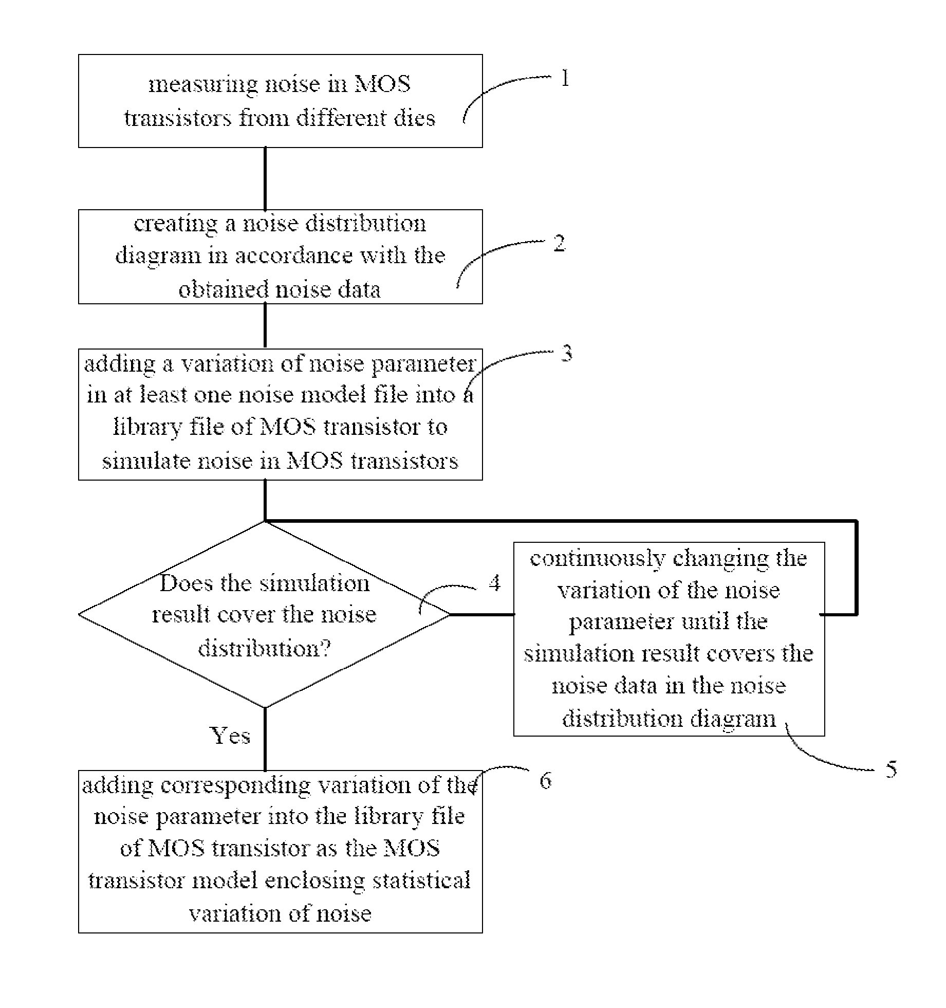
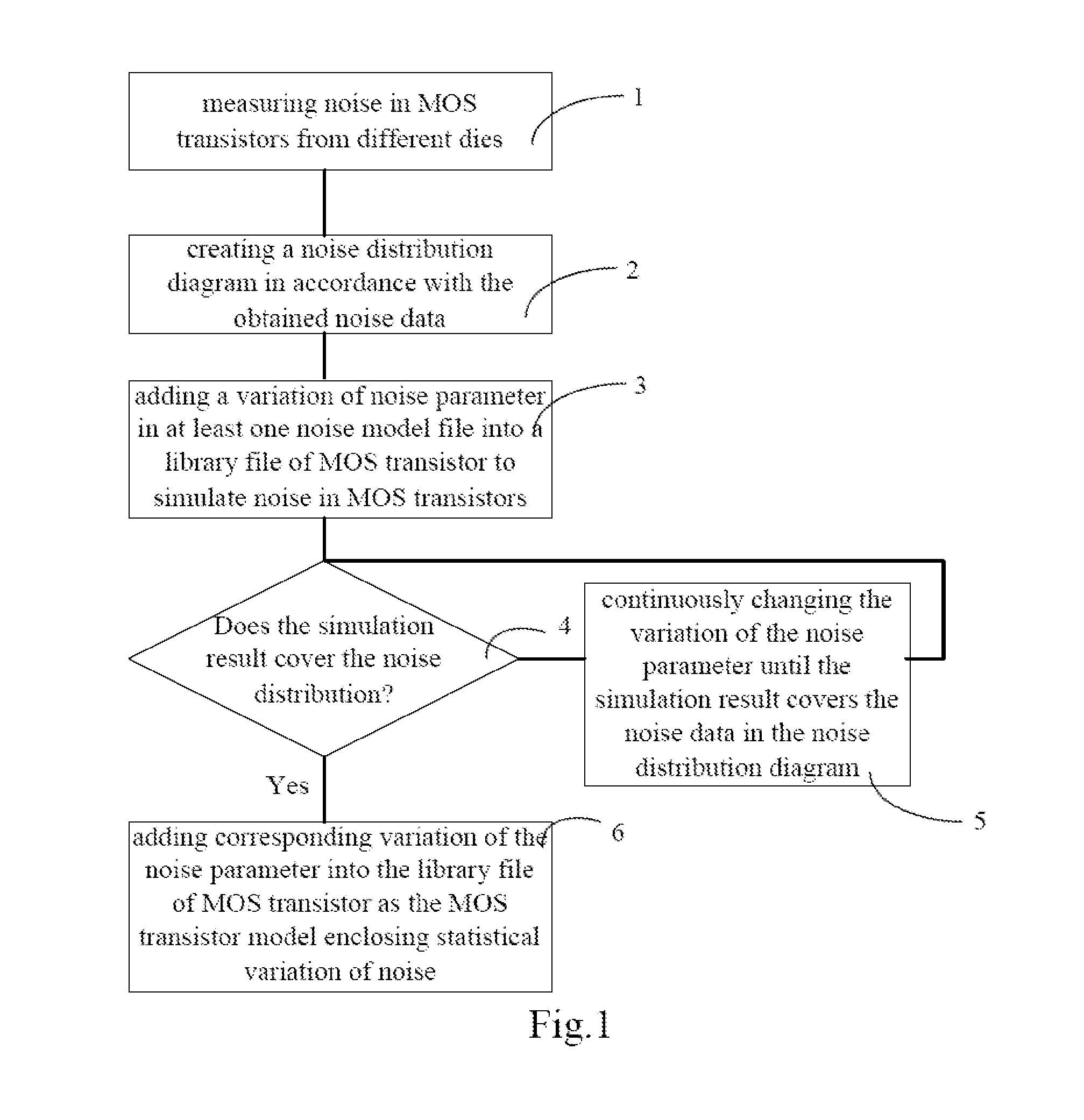
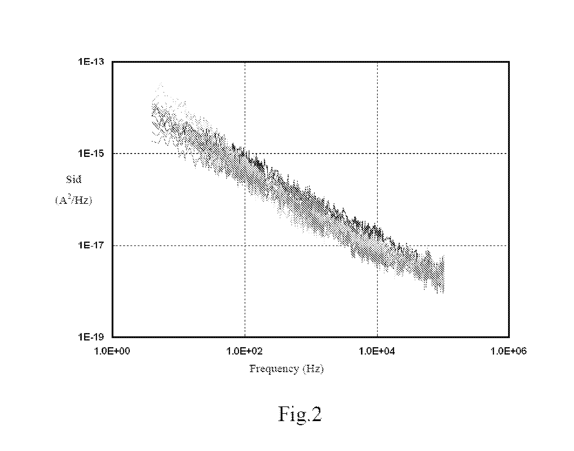
[0032]In accordance with the method for building an MOS transistor model enclosing statistical variation of noise according to the present invention, the measured noise is taken as original data and a distribution diagram is created to describe a statistical distribution of noise. When data in the noise distribution diagram is covered with simulation values of the noise, the model is built.

[0033]In accordance with the method for verifying an MOS transistor model according to the present invention, the measured noise of MOS transistors from different dies is taken as original data and a distribution diagram is created to describe a statistical distribution of noise, the difference in noise character is considered and the difference is used as a criteria for evaluating the precision of a noise model.

[0034]As mentioned above, the noise of an MOS transistor may be divided into numerous categories. Hereinafter, there will be given of descriptions of steps for modeling a noise to make the...


PUM


Abstract

The present invention discloses a method for building an MOS transistor model enclosing statistical variation of noise, including: measuring noise in MOS transistors from different dies; creating a noise distribution diagram in accordance with the obtained noise data of the MOS transistors; adding a variation of noise parameter in at least one noise model file into a library file of MOS transistor to simulate noise in MOS transistors; if a simulation result does not cover the noise data in the noise distribution diagram, changing the variation of the noise parameter until the simulation result covers the noise data in the noise distribution diagram; if the simulation result covers the noise data in the noise distribution diagram, adding corresponding variation of the noise parameter into the library file of MOS transistor as the MOS transistor model enclosing statistical variation of noise. The model obtained by the present invention is more precise.

Description

FIELD OF THE INVENTION[0001]The present invention relates to a method for building an MOS transistor model and a method for verifying an MOS transistor model. In particular, the present invention relates to a method for building an MOS transistor model enclosing statistical variation of noise and a method for verifying an MOS transistor model.BACKGROUND OF THE INVENTION[0002]Currently, devices in a circuit may typically give rise to various noises. For studying the regularity of noise, research is generally made on MOS transistor. The MOS transistor may be considered as a micro circuit, including various resistors, capacitors and active devices. For MOS transistor, thermal noise on gate, source and drain, thermal noise and 1 / f noise in channel, thermal noise on substrate and inductive noise on the gate, etc. may be involved. The 1 / f noise is generally a low frequency noise, and is called like this because the noise increases in inverse proportion to the frequency. The 1 / f noise prim...

Claims


Application Information

Patent Timeline
IPC IPC(8): G06F17/18G06F17/40
CPCG06F17/5036G06F30/367
Inventor HUANG, JUNCHENGZHAO, FANGFANG
Owner SEMICON MFG INT (SHANGHAI) CORP
Why Eureka
Try Eureka