Feature extraction that supports progressively refined search and classification of patterns in a semiconductor layout

a feature extraction and pattern technology, applied in the field of pattern searching, can solve the problems of electrical (parametric) yield problems, present manufacturing difficulties, and significant computing costs of implementing such search functions, and achieve the effect of reducing computational overhead

Inactive Publication Date: 2008-12-25
IBM CORP
View PDF23 Cites 50 Cited by
  • Summary
  • Abstract
  • Description
  • Claims
  • Application Information

AI Technical Summary

Benefits of technology

[0007]A system and method of analyzing shapes to search for patterns in a VLSI layout are disclosed. The system and method allow for the conversion of a layout on several layers to a vector of features, which can be compared to other layouts through standard distance functions. A multi-step process involving partial matching is utilized to reduce computational overhead. The resulting analysis can be used for any purpose, such as causal analysis of systematic defects, the generation of small test cases for optical proximity correction software, etc. Clustering operations may also be utilized to allow, e.g., categories of layout to be discovered through unsupervised learning and passed on to a variety of applications in test, design and analysis.

Problems solved by technology

Due to increasing complexity of lithography, etch, polish and other semiconductor processes, semiconductor manufacturers face a growing challenge in which certain local patterns on one or more design levels present manufacturing difficulties, including fails, electrical (parametric) yield problems, or a small dose-focus process window.
Because the volume of data is very great, the computing cost of implementing such search functions is significant.

Method used


Image

  • Feature extraction that supports progressively refined search and classification of patterns in a semiconductor layout
  • Feature extraction that supports progressively refined search and classification of patterns in a semiconductor layout
  • Feature extraction that supports progressively refined search and classification of patterns in a semiconductor layout

Examples


Embodiment Construction

[0019]As indicated above, the disclosure provides a system, method and program product for performing progressively refined pattern searching that compares vector data collected from a target region with vector data obtained from layout design data. In particular, partial matching is used initially to filter out design patterns that do not match a target pattern. For the purposes of this disclosure, the term “searching” should be interpreted broadly to include, e.g., matching, classifying, grouping, etc.

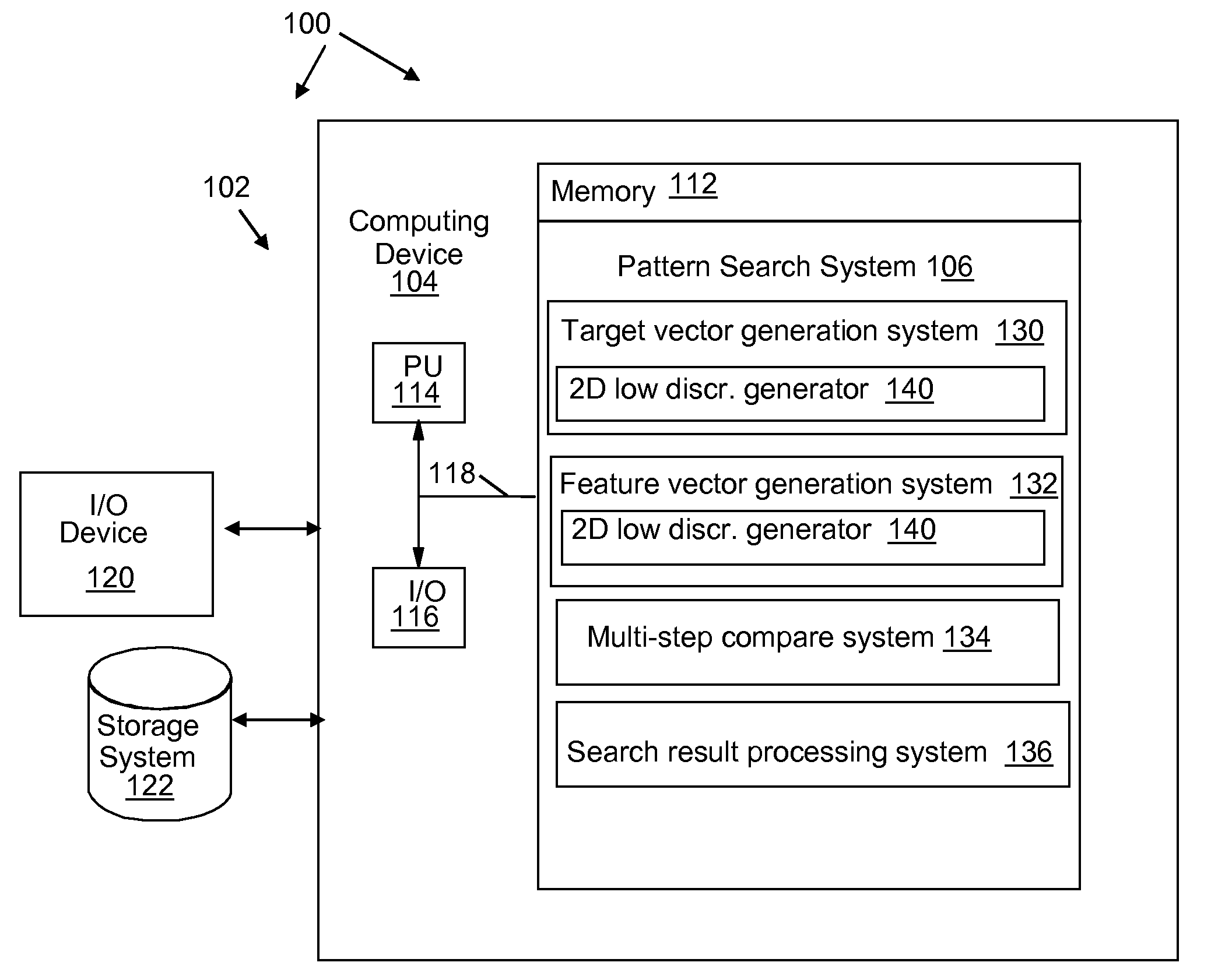
[0020]Turning to the drawings, FIG. 1 shows an illustrative environment 100 for performing pattern searching. To this extent, environment 100 includes a computer infrastructure 102 that can perform the various process steps described herein for performing pattern matching. In particular, computer infrastructure 102 is shown including a computing device 104 that comprises a pattern search system 106, which enables computing device 104 to identify patterns in a VLSI layout by performin...


PUM


Abstract

A system, method and program product for searching and classifying patterns in a VLSI design layout. A method is provided that includes generating a target vector using a two dimensional (2D) low discrepancy sequence; identifying layout regions in a design layout; generating a feature vector for a layout region; comparing a subset of sequence values in the target vector with sequence values in the feature vector as an initial filter, wherein the system for comparing determines that the layout region does not contain a match if a comparison of the subset of sequence values in the target vector with sequence values in the feature vector falls below a threshold; and outputting search results.

Description

BACKGROUND[0001]1. Technical Field[0002]The disclosure relates generally to pattern searching and more particularly to a system and method of performing progressively refined pattern searching and classification that compares vector data collected from a target region with vector data obtained from layout design data.[0003]2. Background Art[0004]Due to increasing complexity of lithography, etch, polish and other semiconductor processes, semiconductor manufacturers face a growing challenge in which certain local patterns on one or more design levels present manufacturing difficulties, including fails, electrical (parametric) yield problems, or a small dose-focus process window.[0005]In addition, elaborate software based resolution enhancement techniques are deployed to improve imaging fidelity on the wafer. New types of design for manufacturing (DFM) software are under development. Testing this software efficiently requires the characterization and classification of typical local lay...

Claims


Application Information

Patent Timeline
Patent Type & Authority Applications(United States)
IPC IPC(8): G06F17/50
CPCG06F17/5081G06F30/398
Inventor DEMARIS, DAVID L.KANJ, ROUWAIDA N.MAYNARD, DANIEL N.MONKOWSKI, MICHAEL D.
Owner IBM CORP
Why Eureka
Try Eureka