Radiation imaging apparatus, method of controlling the same, and radiation imaging system
- Summary
- Abstract
- Description
- Claims
- Application Information
AI Technical Summary
Benefits of technology
Problems solved by technology
Method used
Image

Examples
first exemplary embodiment
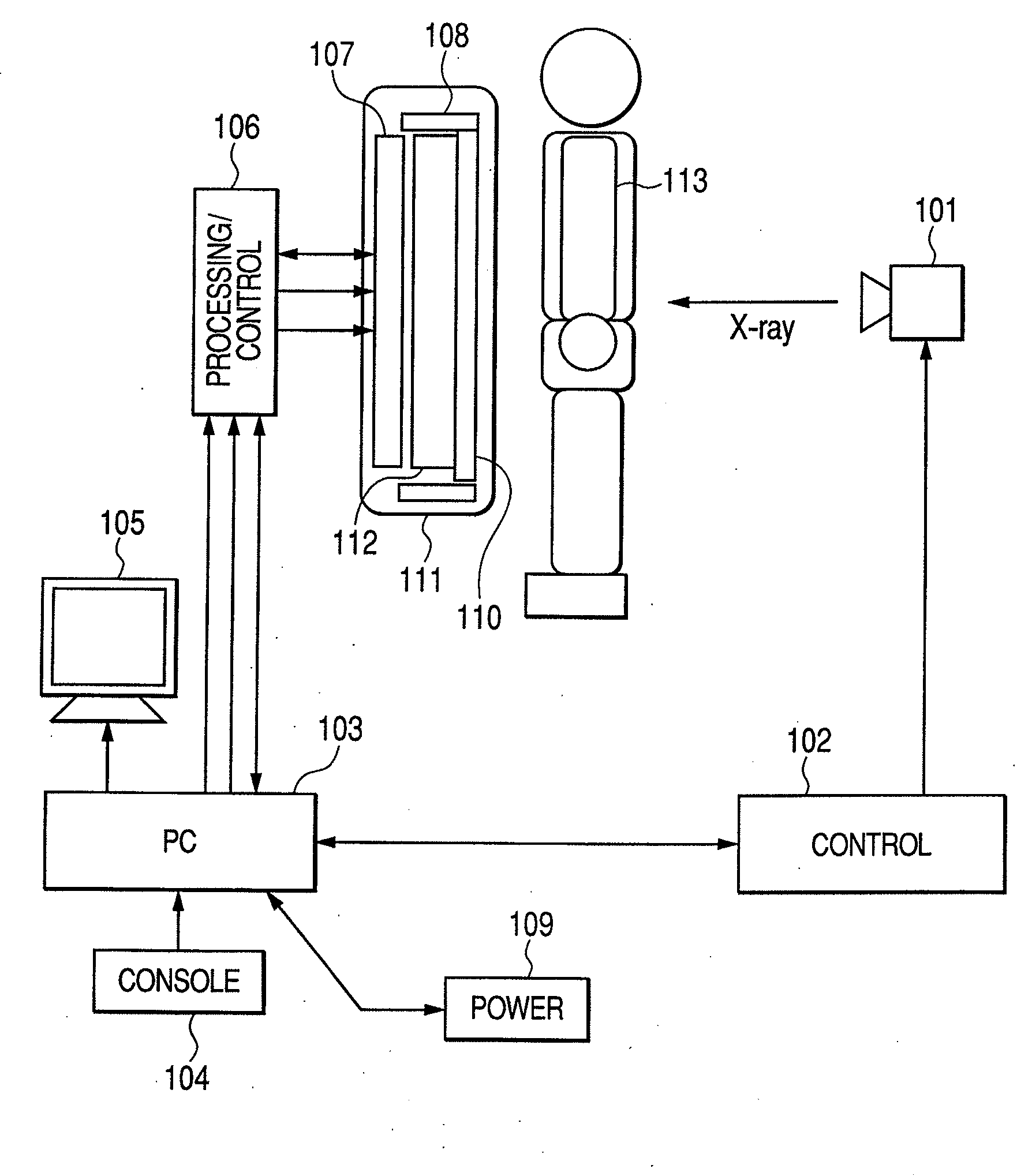
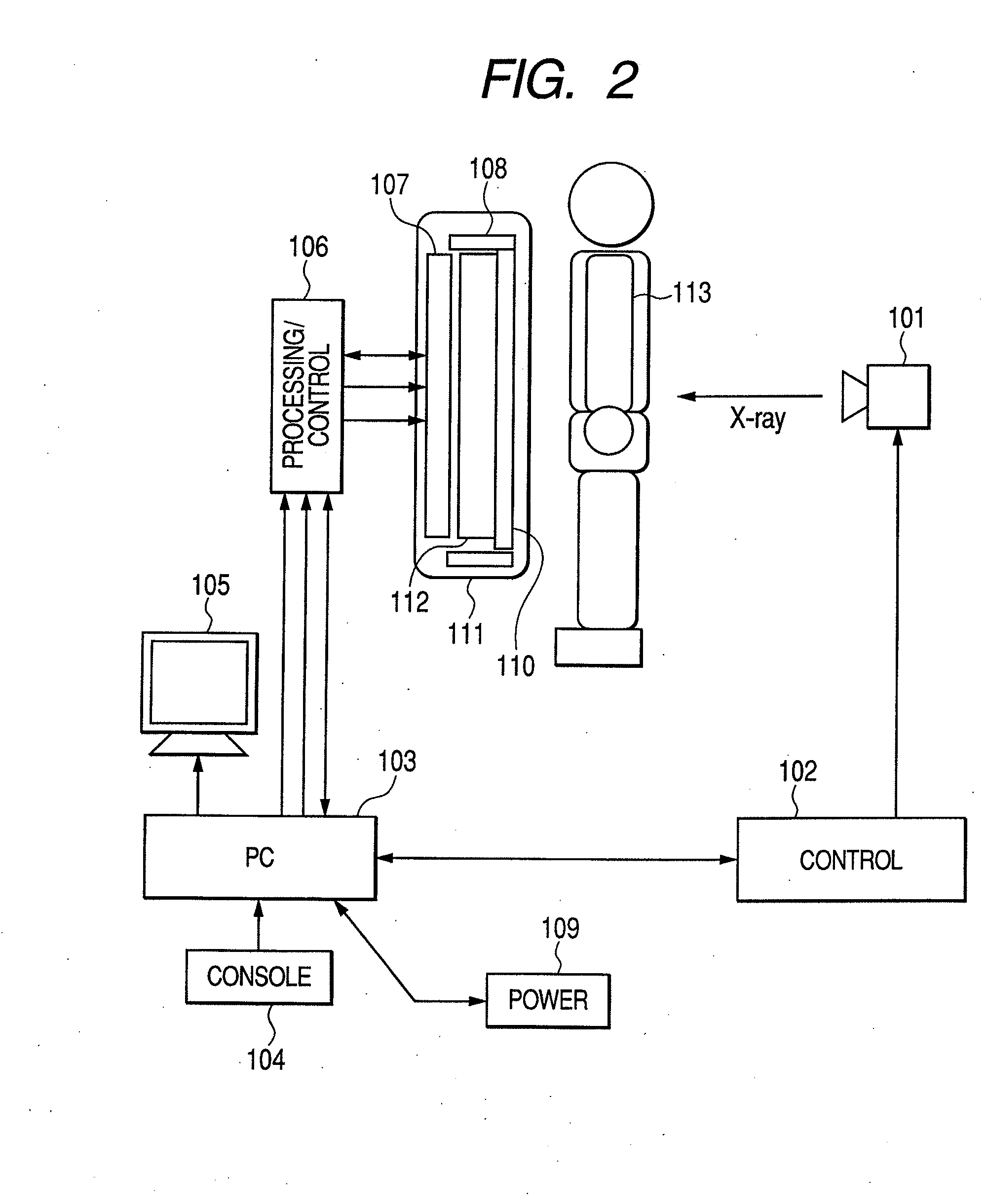
[0032]FIG. 2 is a diagram illustrating an example of the configuration of a digital radiation (X-ray) imaging system according to a first exemplary embodiment of the present invention. This digital radiation imaging system includes an X-ray source 101, an X-ray controller 102, and a digital radiation imaging apparatus. The X-ray source 101 is a radiation generator for generating and irradiating radioactive rays (hereinafter simply referred to as radiation as occasion may demand) (X-rays). The digital radiation imaging apparatus includes a control PC (Personal Computer) 103, a control console 104, a monitor 105, an image processing and control circuit 106, a power supply unit 109, and a flat plane X-ray detector 111. Specifically, the flat plane X-ray detector 111 is a two-dimensional area sensor including a system circuit 107, a read-out circuit 108, a sensor array 110 and a vertical drive circuit 112; and serves to convert radiation into an electric signal to output two-dimensional...
second exemplary embodiment
[0106]FIGS. 8A and 8B are diagrams illustrating an example of the configuration of offset correction unit 602 according to the second exemplary embodiment of the present invention and a processing method therefor. The point of the present embodiment different from the first exemplary embodiment will now be described. The offset correction unit 602 of FIG. 8A differs from the offset correction unit 602 of FIG. 5A in that the offset correction unit 602 is configured by using image memory Mem corresponding to one image and buffer Buf which can hold data corresponding to one line of the flat plane X-ray detector 111. When the input memory switching signal is at High level, switch SW1 connects an output of the flat plane X-ray detector 111 to memory Mem. When the input memory switching signal is at Low level, the switch SW1 connects an output of the flat plane X-ray detector 111 to buffer Buf.
[0107]Moreover, the offset correction unit 602 of FIG. 8A differs from the offset correction uni...
third exemplary embodiment
[0113]FIG. 9 is a circuit diagram illustrating an example of the configuration of flat plane X-ray detector 111 according to the third exemplary embodiment of the present invention, and illustrates a circuit diagram of flat plane X-ray detector 111 using MIS type conversion element 1001 as the conversion element. The point of the present embodiment different from the first exemplary embodiment will now be described. The flat plate X-ray detector 111 includes MIS type conversion elements 1001, transfer TFTs 1002, refreshing TFTs 1003, a refreshing power source 1004, a transfer vertical drive circuit 1005, a refreshing vertical drive circuit 1006, a sensor bias power source 1007, a refreshing line 1008, and sensor bias lines 1009.
[0114]In the MIS type conversion element 1001, as previously described with reference to FIG. 4B, there is the problem that when charges are accumulated at interface between A-Si layer 308 serving as photoelectric conversion layer and insulating layer 307 so ...
PUM
 Abstract
Description
Claims
Application Information
 - R&D
- Intellectual Property
- Life Sciences
- Materials
- Tech Scout
- Unparalleled Data Quality
- Higher Quality Content
- 60% Fewer Hallucinations
Browse by: Latest US Patents, China's latest patents, Technical Efficacy Thesaurus, Application Domain, Technology Topic, Popular Technical Reports.
© 2025 PatSnap. All rights reserved.Legal|Privacy policy|Modern Slavery Act Transparency Statement|Sitemap|About US| Contact US: help@patsnap.com