Accurate Capacitance Measurement for Ultra Large Scale Integrated Circuits

a capacitance measurement and ultra-large-scale technology, applied in semiconductor/solid-state device testing/measurement, semiconductor/solid-state device details, instruments, etc., can solve problems such as poor accuracy, incomplete parametric capacitance associated with contacts, and inability to accurately estimate existing extraction methods, etc., to achieve the effect of improving accuracy

Active Publication Date: 2009-01-01
TAIWAN SEMICON MFG CO LTD
View PDF36 Cites 75 Cited by
  • Summary
  • Abstract
  • Description
  • Claims
  • Application Information

AI Technical Summary

Benefits of technology

[0013]An advantage of a preferred embodiment of the present invention is that parasitic capacitance associated with contact and via in an IC can be measured with substantially improved accuracy. This is achieved by eliminating the effects of the not-to-be-measured capacitances from the me

Problems solved by technology

This trend poses continuous technical challenges in manufacturing ICs with improved performance.
However, the parasitic capacitance associated with the contacts and vias, which are formed in an IC to couple a net with a device node and to connect nets in different interconnect layers, is either ignored or estimated with poor accuracy.
When the trend of device scaling in an IC continues, the existing extraction methodology is problematic for various reasons.
Firstly, contact and via capacitance accounts for a significantly increased proportion of the total interconnect delay in ICs made with advanced technology, due to the reduced contact-to-gate-electrode spacing

Method used


Image

  • Accurate Capacitance Measurement for Ultra Large Scale Integrated Circuits
  • Accurate Capacitance Measurement for Ultra Large Scale Integrated Circuits
  • Accurate Capacitance Measurement for Ultra Large Scale Integrated Circuits

Examples


Embodiment Construction

[0033]The making and using of the presently preferred embodiments are discussed in detail below. It should be appreciated, however, that the present invention provides many applicable inventive concepts that can be embodied in a wide variety of specific contexts. The specific embodiments discussed are merely illustrative of specific ways to make and use the invention, and do not limit the scope of the invention.

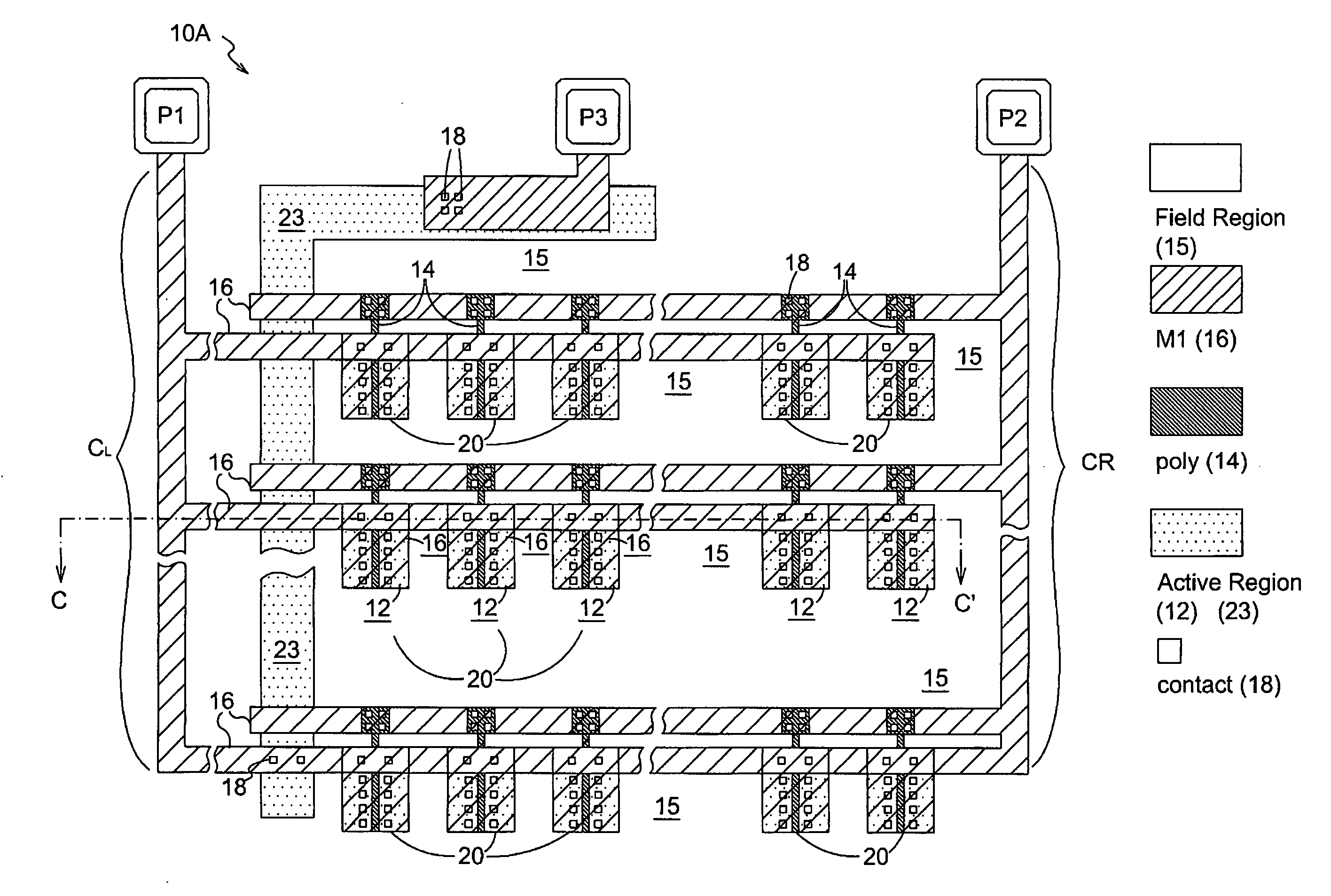
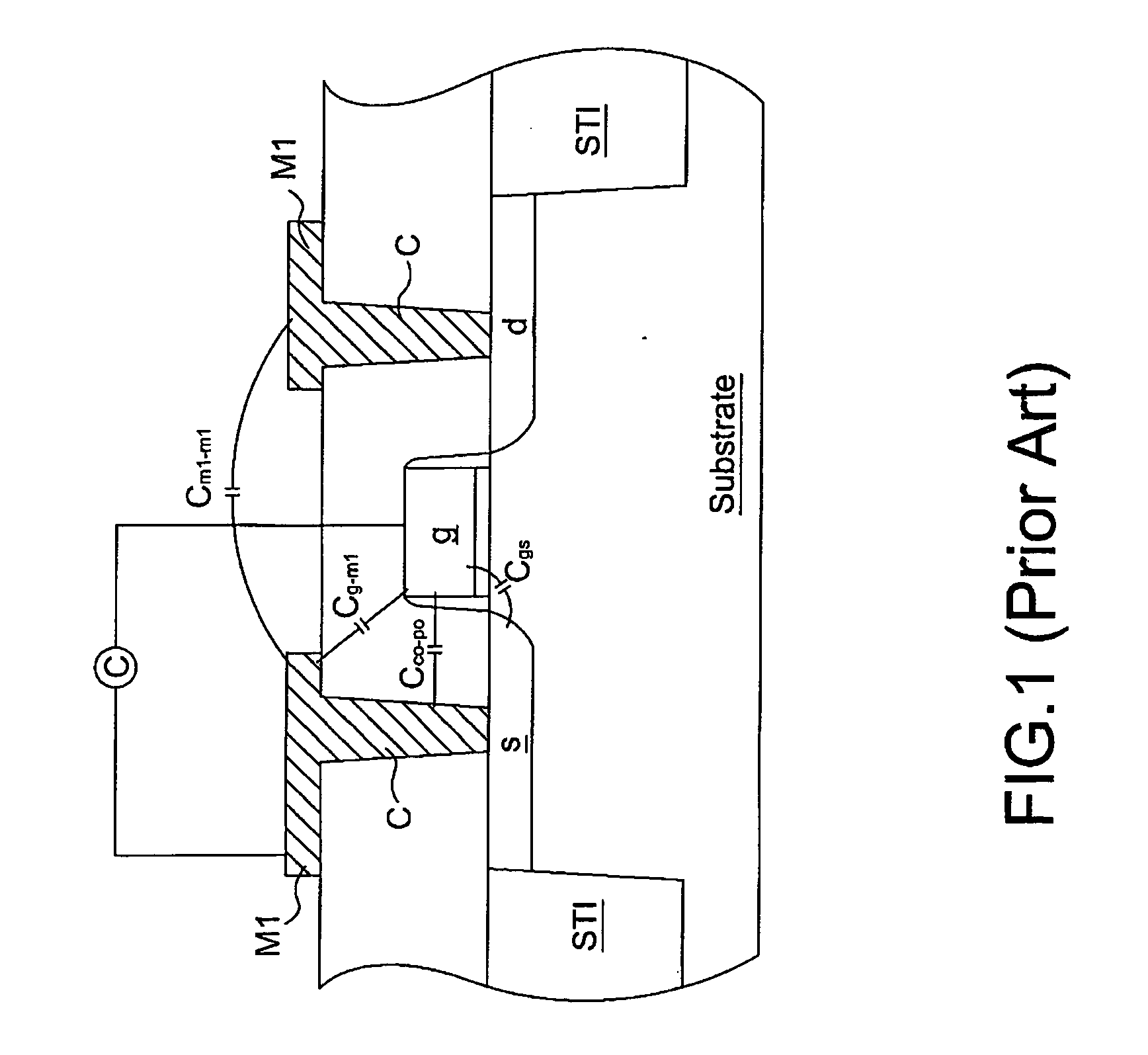
[0034]The present invention will be described with respect to preferred embodiments in a specific context, namely contact and via capacitance test structures and methods of conducting contact and via capacitance measurement in an IC. A common feature of the various embodiments of the current invention is to eliminate the not-to-be-measured capacitances from the measurement results through proper design on test structures and measuring procedures. Contact and via capacitance measurements made by preferred test structures and methods result in significantly improved measurement...


PUM


Abstract

Test structures and methods for measuring contact and via parasitic capacitance in an integrated circuit are provided. The accuracy of contact and via capacitance measurements are improved by eliminating not-to-be-measured capacitance from the measurement results. The capacitance is measured on a target test structure that has to-be-measured contact or via capacitance. Measurements are then repeated on a substantially similar reference test structure that is free of to-be-measured contact or via capacitances. By using the capacitance measurements of the two test structures, the to-be-measured contact and via capacitance can be calculated.

Description

[0001]This application claims the benefit of U.S. provisional application No. 60 / 947,269, filed on Jun. 29, 2007, entitled “Method and System to Enable Design Optimization of Via and Contact,” which application is hereby incorporated herein by reference.CROSS-REFERENCE TO RELATED APPLICATIONS[0002]This application relates to the following co-pending and commonly assigned patent application Ser. No. 11 / 865,304 filed on Oct. 1, 2007, entitled “Accurate Parasitic Capacitance Extraction for Ultra Large Scale Integrated Circuits” (TSM07-0376), which application is hereby incorporated herein by reference.TECHNICAL FIELD[0003]The present invention relates generally to techniques of parametric measurements in an integrated circuit, and more particularly, to on-chip test structures, and corresponding method of measuring contact and via parasitic capacitance in a semiconductor device.BACKGROUND[0004]As the density of integrated circuits continues to increase, the scaling down of the semicondu...

Claims


Application Information

Patent Timeline
IPC IPC(8): G01R31/26H01L23/58
CPCG01R31/2853G01R31/2884H01L22/34H01L2924/0002H01L2924/00
Inventor DOONG, YIH-YUHCHANG, KEH-JENGMII, YUH-JIERLIU, SALLYHUNG, LIEN JUNGCHANG, VICTOR CHIH YUAN
Owner TAIWAN SEMICON MFG CO LTD
Why Eureka
Try Eureka