Screen input type image display

a display device and input type technology, applied in the field of screen input type image display, or display device, can solve the problems of increasing the number of manufacturing processes and complicated structures, and achieve the effect of high precision and simple structur

Inactive Publication Date: 2009-01-01
JAPAN DISPLAY INC
View PDF14 Cites 84 Cited by
  • Summary
  • Abstract
  • Description
  • Claims
  • Application Information

AI Technical Summary

Benefits of technology

[0014]An object of the present invention is to provide an image display device incorporating a touch sensor capable of detecting coordinates with a simple structure and high precision.

Problems solved by technology

As a result, the structure becomes complicated and the number of manufacturing processes becomes more than that in a simple structure described in Patent Document 1.

Method used


Image

  • Screen input type image display
  • Screen input type image display
  • Screen input type image display

Examples


first embodiment

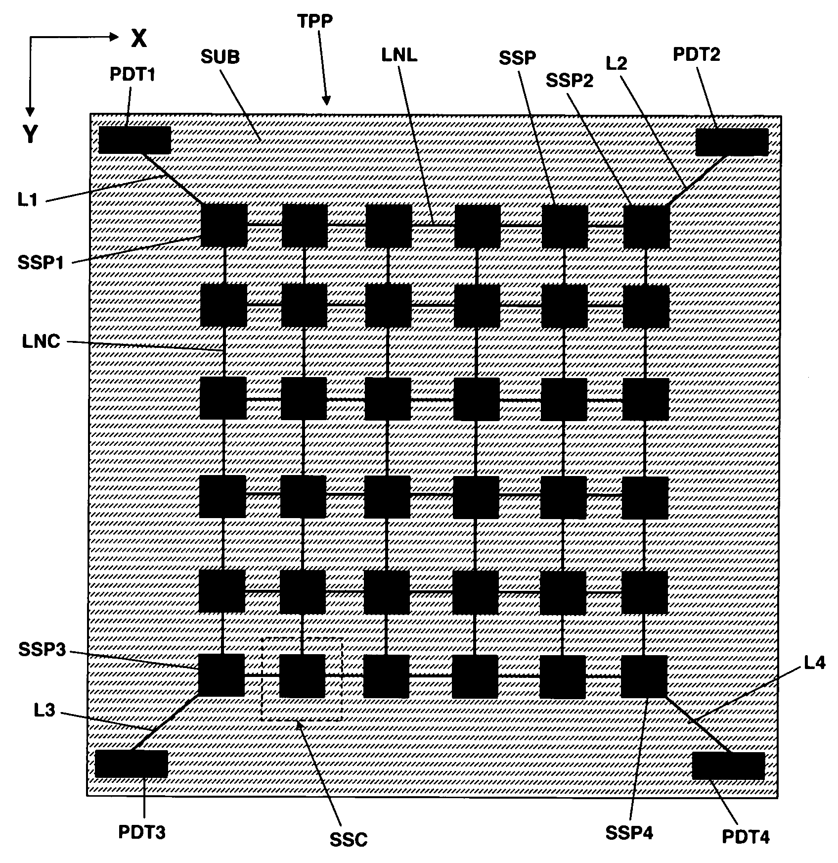
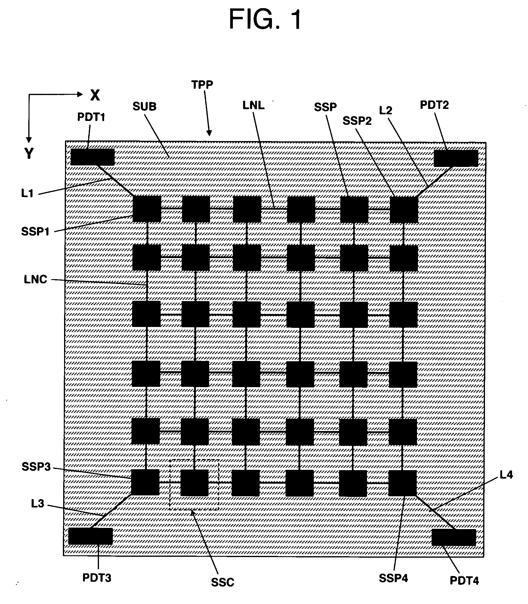
[0048]FIGS. 1 to 4 are diagrams for explaining a first embodiment of the present invention. FIG. 1 is a plan view of a principal part of a touch sensor for explaining the first embodiment of the present invention. This touch sensor includes a touch panel TPP for detecting a position of an input from the outside in an operation plane which spreads in an X direction (row direction) and a Y direction (column direction) by using a static capacitive coupling scheme. This touch sensor is a touch sensor which detects an input point from external in an operation plane (touch input plane) spreading in the X direction and the Y direction.

[0049]The touch panel TPP is formed by arranging a plurality of pad electrodes SSP obtained by patterning a transparent conductive film for which the ITO is suitable, and row connection electrodes LNL and column connection electrodes LNC which connect the pad electrodes SSP to each other, on a surface of a substrate SUB so as to form a two-dimensional matrix....

second embodiment

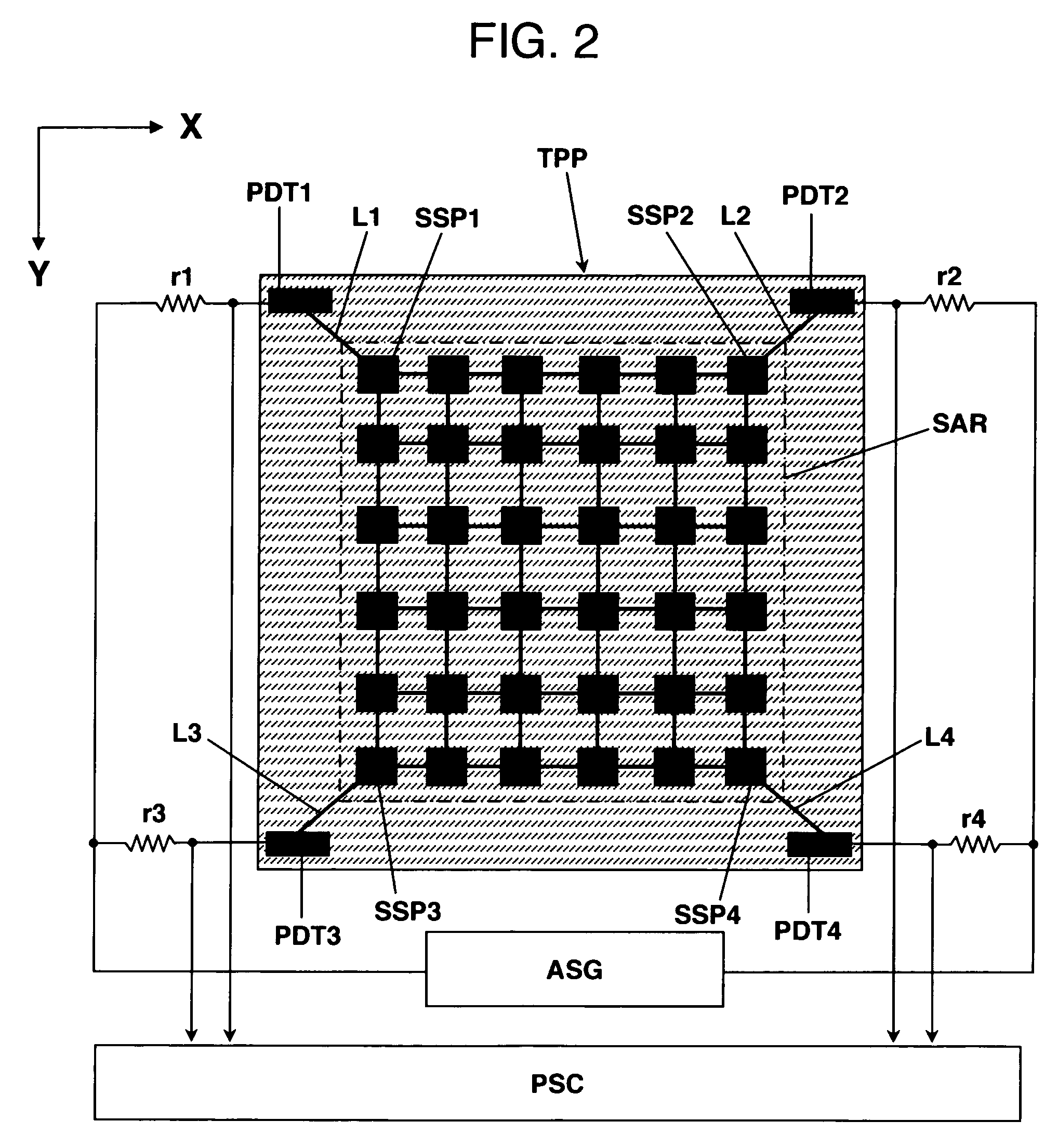
[0054]FIG. 5 is a plan view of a principal part for explaining a second embodiment of the present invention in the same way as FIG. 1. The same reference characters as those in FIG. 1 denote like functional parts, and in principle duplicate description of them will be omitted. In addition to the pad electrodes SSP, the row connection electrodes LNL and the column connection electrodes LNC in the first embodiment, row spine electrodes LNLB and column spine electrodes LNCB for mutually connecting only the row connection electrodes LNL and the column connection electrodes LNC are included in the second embodiment. And a row spine electrode LNLB and a column spine electrode LNCB on outermost sides of the matrix, and coordinate detection terminals PDT1 to PDT4 are connected by wires L1 to L4.

[0055]According to the configuration according to the second embodiment, the row spine electrodes LNLB and column spine electrodes LNCB in addition to the detection cell SSC constitute current paths....

third embodiment

[0056]FIG. 6 is a plan view of a principal part of a touch panel for explaining a third embodiment of the present invention. The same reference characters as those in FIGS. 1 and 5 denote like functional parts, and in principle duplicate description of them will be omitted. In the third embodiment, pad electrodes located on four corners of a fringe of a detection area are electrically connected to coordinate detection terminals PDT1 to PDT4 provided on four corners of the substrate via wires L1 to L4 each formed of a transparent conductive film or a metal film. Electrode widths of the row connection electrodes LNL and the column connection electrodes LNC which connect detection cells SSC of the matrix are made wider in the center part than in the peripheral part. The electrode widths of the row connection electrodes LNL and the column connection electrodes LNC are made gradually wide from the peripheral part toward the central part so as to become the minimum in the peripheral part ...


PUM


Abstract

In an image display device incorporating a touch sensor capable of detecting coordinates with simple structure and high precision, a transparent conductive film on a substrate SUB forming a display screen of the image display device is patterned to form detection electrodes taking the shape of a plurality of pad electrodes SSP arranged in a two-dimensional matrix form of rows (X direction) and columns (Y direction). Row connection electrodes LNL and column connection electrodes LNC connecting the detection electrodes in rows and columns of the two-dimensional matrix to each other are formed of the same transparent conductive film as the pad electrodes. By arranging the pad electrodes in the matrix form, the contact area of a finger or the like touching the screen can be made large, resulting in improved detection precision (resolution). The pad electrodes are connected at four corners to coordinate detection terminals PDT1 to PDT4.

Description

INCORPORATION BY REFERENCE[0001]The present application claims priority from Japanese application JP2007-169031 filed on Jun. 27, 2007, the content of which is hereby incorporated by reference into this application.BACKGROUND OF THE INVENTION[0002]The present invention relates to a screen input type image display, or display device. In particular, the present invention is suitable for raising the coordinate detection precision in an image display device having a touch sensor of capacitive coupling scheme.[0003]Image display devices including touch sensors having a screen input function of inputting information by touch operation (hereafter referred to simply as touch) of a user's finger or the like with a display screen are used in mobile electronic devices such as PDAs and potable terminals, various home electronic products, and stationary customer guide terminals such as unattended reception devices. As image display devices having such a touch input function, a scheme of detectin...

Claims


Application Information

Patent Timeline
Patent Type & Authority Applications(United States)
IPC IPC(8): G06F3/045
CPCG06F3/045G06F3/044G06F3/0412G06F3/0444
Inventor KINOSHITA, MASAYOSHIMAMBA, NORIO
Owner JAPAN DISPLAY INC
Why Eureka
Try Eureka