[0009]Accordingly, it is an object of the present invention to provide a method of
machining a wafer by which it is possible, in a process of manufacturing a device such as a
semiconductor chip having penetrating electrodes, to secure rigidity of a wafer thinned before splitting into individual devices, to facilitate handling of the thin wafer, to thereby enable smooth transfer of the wafer between
processing steps, and, at the stage of wafer, to easily and securely obtain a condition where an insulating film is formed in the surroundings of top portions of the penetrating electrodes exposed on the back side, so as thereby to realize enhanced productivity and yield.
[0011]According to the present invention, in the back side recessed part forming step, the back-side surface portion corresponding only to the device formation region needing
thinning is thinned by
grinding, whereas the surrounding outer
peripheral marginal region is left in its original thickness so as to form the annular projected part, to thereby obtain a wafer which has been thinned and yet the rigidity of which is secured with the annular projected part. Therefore, the transferring of the wafer between
processing steps after the back side recessed part forming step and the handling of the wafer in the
processing steps themselves are rendered safe and easy, and a lowering in the yield due to
cracking of the wafer can be prevented from occurring. In addition, the wafer after completion of the back side recessed part
cutting step conducted as the final step in the method according to the present invention is transferred to a splitting step for splitting the wafer into individual devices, and the wafer transferring and splitting operations in this process can also be progressed safely and easily, resulting in enhanced productivity and yield of the device.
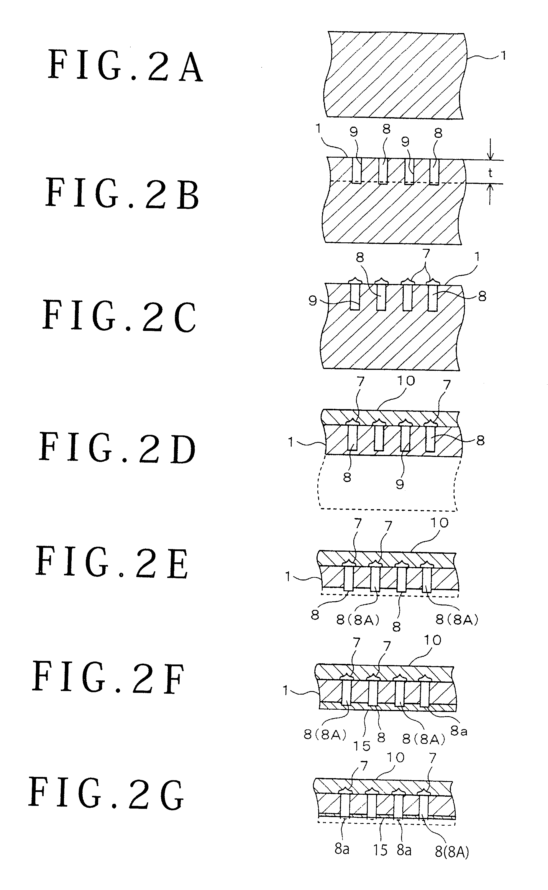
[0012]In the present invention, the back side
electrode parts are formed by causing the metallic electrodes to project from the bottom surface of the recessed part on the back side of the wafer in the
etching step, whereby the metallic electrodes are made to constitute penetrating electrodes. Then, the recessed part is coated with the resin in the subsequent insulating film forming step to form the insulating film, and thereafter the insulating film and the back side electrodes are flattened by
cutting, whereby a condition is obtained on the back side of the wafer in which the insulating film is formed in the surroundings of the top portions of the penetrating electrodes. According to the present invention, not only the resin is applied to the back side on which the penetrating electrodes (back side electrode parts) are projecting, but also the resin is flattened by
cutting together with the back side electrode parts after the application of the resin. Therefore, the back side electrode parts are securely exposed, and the insulating film is formed in the surroundings of the back side electrode parts so as to be flush with the latter, resulting in that defective conduction can be prevented from occurring upon mounting of each of the devices.
[0014]According to the present invention, the
thinning of the wafer by grinding the back-side surface is applied only to the region corresponding to the device formation region so as to form the surrounding outer
peripheral marginal region into the thick annular projected part, whereby rigidity of the wafer can be secured, resulting in that the thin wafer can be easily handled and can be smoothly transferred between processing steps. In addition, it is possible to assuredly form the wafer back side in the condition in which the insulating film is formed in the surroundings of the top portions of the back-side electrode parts exposed. As a result of the foregoing, an enhancing effect on the productivity and the yield is promised.

