Solid-state imaging device and method for fabricating the same

a solid-state imaging and imaging device technology, applied in the direction of radiological control devices, instruments, television systems, etc., can solve the problems of difficult to obtain a lens curved face having a smooth and uniform shape after heat flow, and the sensitivity is reduced as compared, so as to achieve high light receiving efficiency and great thickness

Active Publication Date: 2009-01-08
GK BRIDGE 1
View PDF5 Cites 40 Cited by
  • Summary
  • Abstract
  • Description
  • Claims
  • Application Information

AI Technical Summary

Benefits of technology

[0008]First, unlike a CCD image sensor, a MOS image sensor generally includes a plurality of layers of metal interconnects formed over a photoelectric conversion portion for converting incident light into an electric charge. Therefore, if a focal point is situated below an upper face of a substrate, the incident light is easily scattered or reflected by the interconnects, which lowers the sensitivity as compared to the case where the focal point is adjusted to be on the upper face of the substrate. That is, if a focal position is situated below the upper face of the substrate 111, the amount of light reflected by the metal interconnects increases, and thus the light collection efficiency to a photodiode lowers.
[0011]Therefore, an object of the present invention is to provide a solid-state imaging device in which a deterioration of a sensitivity characteristic with respect to a diaphragm (F value) characteristic of an imaging device (camera) is small, with the sensitivity characteristic being improved.
[0013]With this configuration, the effective refractive index of each second lens can be lower as compared to the case where the transparent film is not provided. Therefore, a focal position of light passing through the second lens can be optimized easily. For example, even in the case where the second lens is formed by an organic material such as a photoresist, a focal position of incident light can be situated above the semiconductor substrate while the second lens has a great thickness.
[0015]With this method, it is possible to form a solid-state imaging device having a high light receiving efficiency.
[0016]Specifically, the second lenses are preferably formed of an organic material such as a photoresist, because in this case, an upward or downward convexly curved face can be formed easily. In this case, the patterns formed of the organic material are heated, so that the second lenses can be formed. Here, the patterns may have a sufficiently great thickness, and at the same time, a focal point of light passing through each second lens and each first lens can be situated above the upper face of the semiconductor substrate.

Problems solved by technology

However, the solid-state imaging device according to the conventional technique has problems as follows.
Therefore, if a focal point is situated below an upper face of a substrate, the incident light is easily scattered or reflected by the interconnects, which lowers the sensitivity as compared to the case where the focal point is adjusted to be on the upper face of the substrate.
However, in the heat reflow process for forming the lenses 128, if the height (thickness) of the rectangular patterns is smaller (thinner) than a certain height (thickness), an upper face of a center portion of each lens 128 is flat as shown in FIG. 17B, and thus it is difficult to obtain a lens curved face having a smooth and uniform shape after heat flow.
Therefore, in the conventional solid-state imaging device, the shape of the top lens may not be formed as it is designed.

Method used


Image

  • Solid-state imaging device and method for fabricating the same
  • Solid-state imaging device and method for fabricating the same
  • Solid-state imaging device and method for fabricating the same

Examples


embodiment 1

Variation of Embodiment 1

[0093]Next, with reference to FIGS. 10 and 11, detailed descriptions will be given of a solid-state imaging device (MOS image sensor) according to a variation of Embodiment 1.

[0094]FIGS. 10A and 10B are views showing longitudinal sections respectively along the horizontal direction and the diagonal direction of part of a pixel of a MOS image sensor according to the variation of Embodiment 1. FIGS. 11A, 11B, and 11C are plan views respectively showing an interconnect pattern of the first layer, an interconnect pattern of the second layer, and an interconnect pattern of the third layer of part of the pixel of the MOS image sensor according to the variation of Embodiment 1. Here, as a rule, “diagonal direction” means, in the case where the imaging area is a quadrilateral in a plan view, a diagonal direction of the quadrilateral.

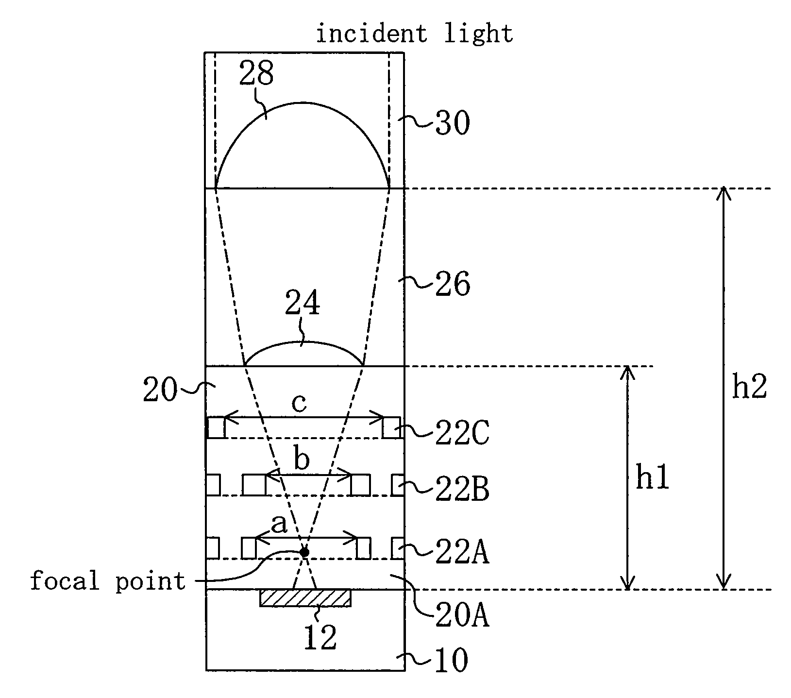
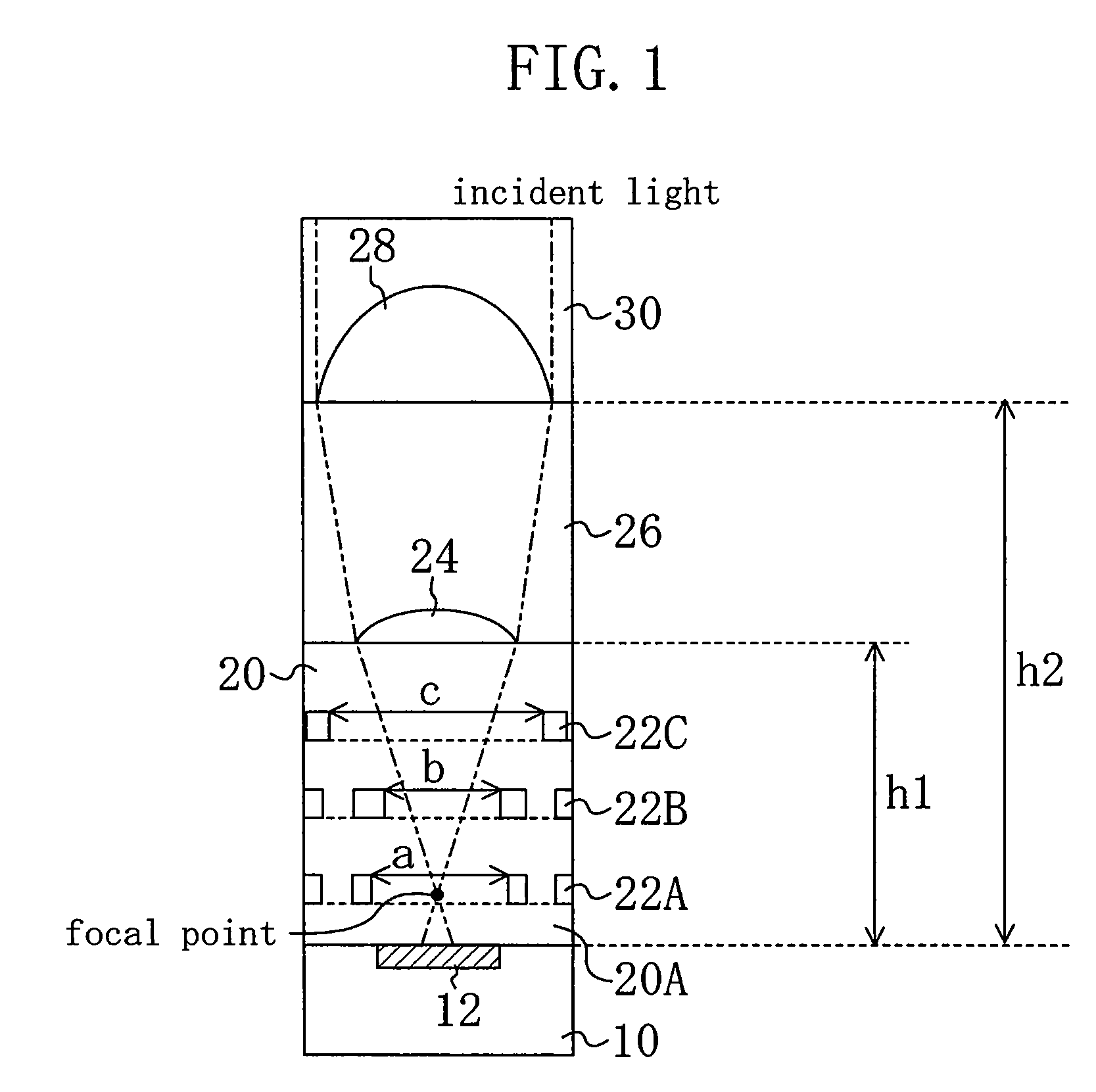
[0095]In the MOS image sensor of FIG. 1 according to Embodiment 1, in longitudinal sections taken along any direction, the focal positi...

embodiment 2

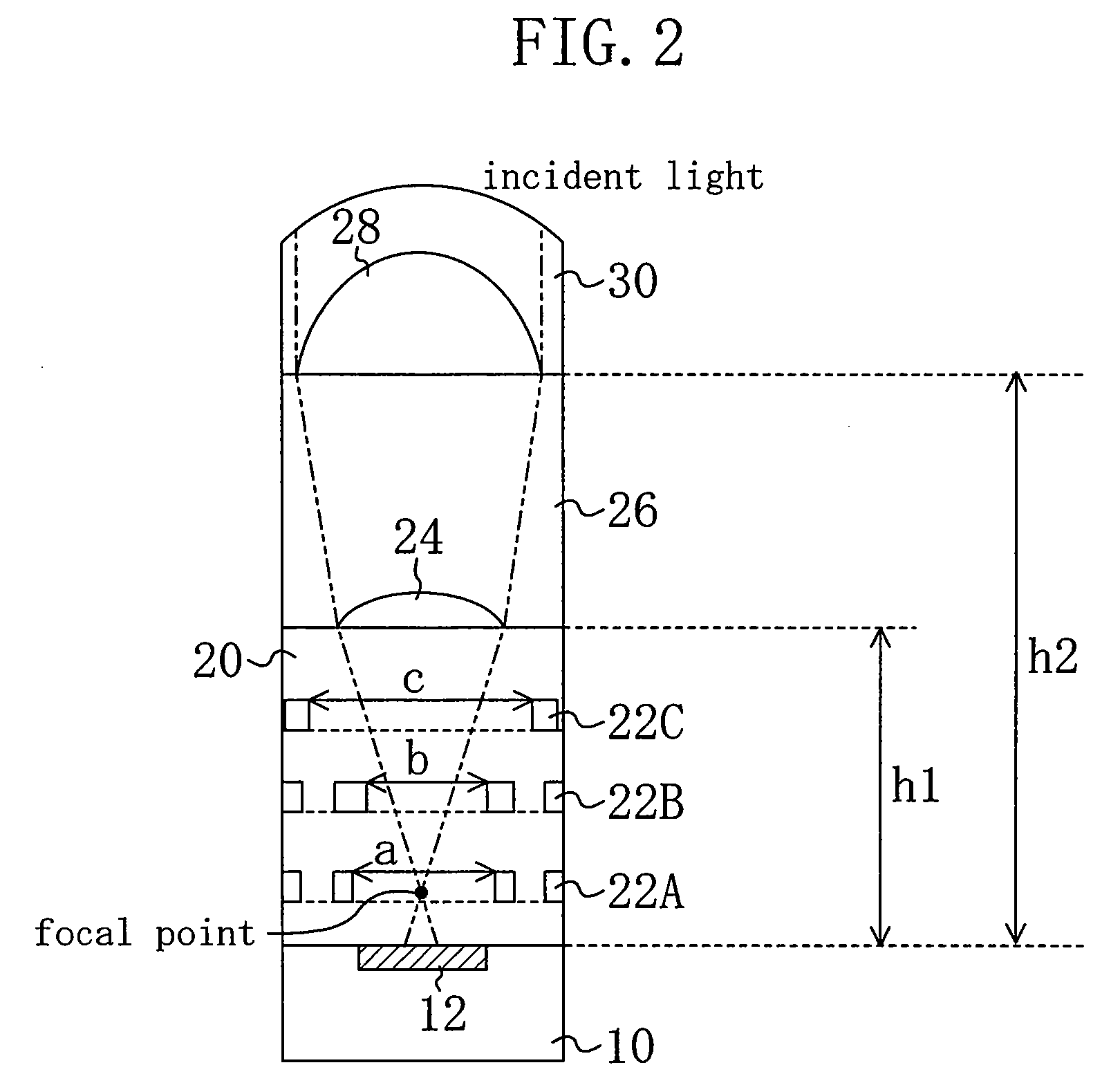
[0108]FIG. 14 is a cross-sectional view showing part of a pixel of a MOS image sensor according to Embodiment 2 of the present invention. In the figure, members which are the same as those in the MOS image sensor of FIG. 1 of Embodiment 1 are denoted by the same reference numbers as those in FIG. 1.

[0109]As shown in FIG. 14, the MOS image sensor of the present embodiment is different from the MOS image sensor of Embodiment 1 in that a lower face of an inner-layer lens 25 is downward convex (is concave).

[0110]In this case, a distance h3 between an upper face of the semiconductor substrate 10 and the inner-layer lens 25 is substantially the same as the distance h1 of the MOS image sensor of Embodiment 1. However, a distance h4 between the upper face of the semiconductor substrate 10 and the top lens 28 can be smaller than the distance h2 of the MOS image sensor of Embodiment 1.

[0111]The reason for this is that if an upper face of the inner-layer lens is convex, the inner-layer lens 24...


PUM


Abstract

A solid-state imaging device includes: an imaging area in which light receiving portions are disposed; an interconnect layer disposed on the light receiving portions, the interconnect layer including metal interconnects having openings and first insulating films; inner-layer lenses formed over the interconnect layer in one-to-one relationship with the light receiving portions; a transparent second insulating film formed on the interconnect layer and the inner-layer lenses; top lenses formed on the second insulating film in one-to-one relationship with the light receiving portions, an upper face of each of the top lenses being a convexly curved face; and a transparent film on the top lenses, the transparent film being formed of a material having a refractive index smaller than a refractive index of the top lenses. In this way, a focal point of at least part of incident light can be situated above a semiconductor substrate.

Description

BACKGROUND OF THE INVENTION[0001]1. Field of the Invention[0002]The present invention relates to a solid-state imaging device including lenses provided above a semiconductor substrate on which light receiving portions such as photoelectric conversion portions are formed, the lenses guiding incident light to the light receiving portions.[0003]2. Description of the Prior Art[0004]Generally, a solid-state imaging device such as a MOS image sensor is structured such that over a semiconductor substrate having a light receiving portion (a photoelectric conversion portion such as a photodiode), a variety of films such as a light-shielding pattern and an interconnect pattern is disposed in multi-layered manner. When such a solid-state imaging device is downsized, the exit pupil distance of a camera lens necessarily shortens. This increases an oblique component of light entering a pixel array portion (imaging area), especially the periphery of the pixel array portion, wherein in the pixel ar...

Claims


Application Information

Patent Timeline
Patent Type & Authority Applications(United States)
IPC IPC(8): H01L33/00H01L21/00H01L27/14H01L27/146H01L31/10H04N5/335H04N5/369
CPCH01L27/14623H01L27/14636H01L27/14627
Inventor KATSUNO, MOTONARIMIYAGAWA, RYOHEI
Owner GK BRIDGE 1
Why Eureka
Try Eureka