Semiconductor device and semiconductor device manufacturing method

Inactive Publication Date: 2009-01-08
PS4 LUXCO SARL
View PDF5 Cites 14 Cited by
  • Summary
  • Abstract
  • Description
  • Claims
  • Application Information

AI Technical Summary

Benefits of technology

[0034]According to the invention, the contact plug includes a small-diameter part and a large-diameter part arranged on the small-diameter part, the outer diameter of the large-diameter part is larger than the outer diameter of the small-diameter part, and the outer diameter of the large-diameter part is larger than the outer diameter of a connection face between the second conductive member and the large-diameter part. This reduces the outer diameter of the small-diameter part and allows the semiconductor device to be miniaturized.
[0035]Moreover, according to the invention, the large-diameter part of the contact plug is larger than the outer diameter of the small-diameter part, and the outer diameter of the large-diameter part is larger than the outer diameter of a connection face between the second conductive member and the large-diameter part. This makes it possible to maintain an adequate contact area between the second conductive member and the contact plug. As a result, contact resistance between the second conductive member and the contact plug can be reduced; in addition, current is unlikely to constrict in the connection section between the second conductive member and the contact plug, whereby increase of leak current caused by current constriction can be reduced.
[0036]Further, according to the invention, the outer diameter of the large-diameter part of the contact plug is larger than the outer diameter of a connection face between the second conductive member and the large-diameter part. This can prevent the second conductive member from missing the contact plug when the second conductive member is being formed.
[0037]The semiconductor device manufacturing method of the embodiment of the invention includes: forming, on the first interlayer insulating film, a first resist mask exposing a small-diameter part formation region where the small-diameter part is formed; etching the first interlayer insulating film of the small-diameter part formation region to form a first capacitor contact hole having a bottom face exposed at a first conductive member; removing the first resist mask; forming, on the first interlayer insulating film, a second resist mask exposing a large-diameter part formation region where the large-diameter part will on the first interlayer insulating film is formed; etching the first interlayer insulating f

Problems solved by technology

This has led to a problematic decrease in the amount of charge accumulated in the capacitor.
However, as semiconductor devices become more miniaturized and thinner, it is becoming difficult to employ SAC etching in forming a capacitor contact hole.
However, even when using these conventional techniques, since the area of contact between the capacitor lower electrode and the capacitor contact plug is decreasing as semiconductor device become more miniaturized and thinner, the follow

Method used


Image

  • Semiconductor device and semiconductor device manufacturing method
  • Semiconductor device and semiconductor device manufacturing method
  • Semiconductor device and semiconductor device manufacturing method

Examples


Example

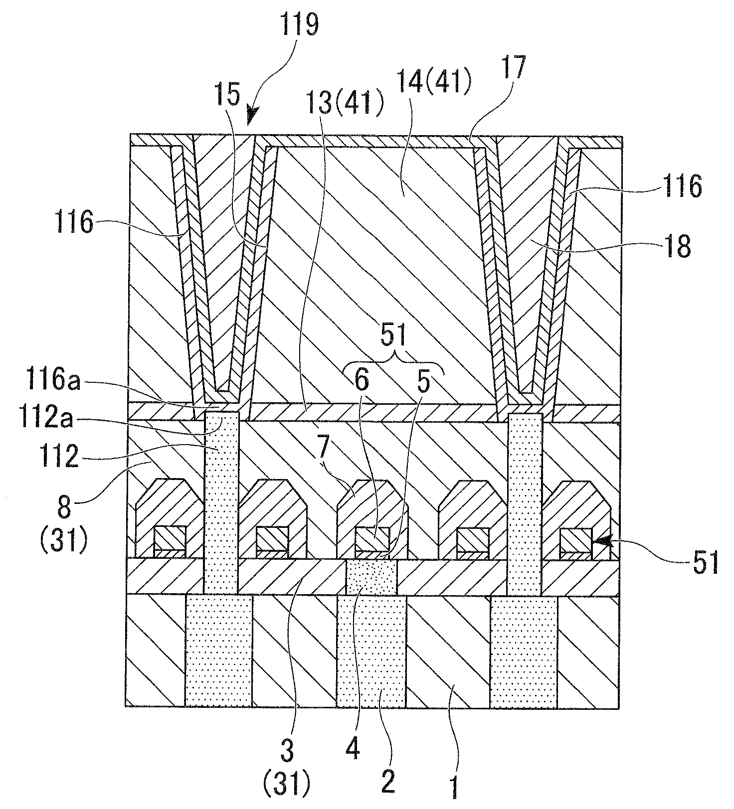
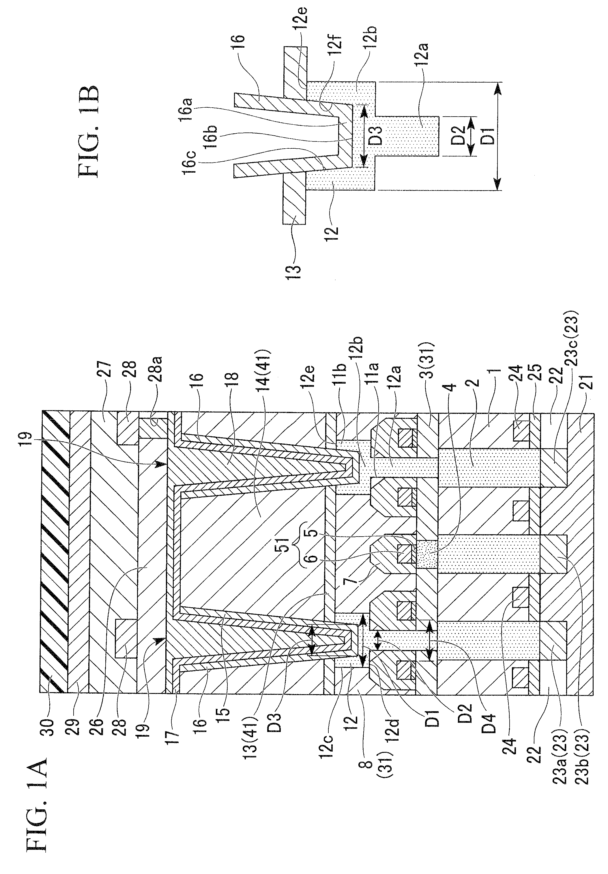
[0052]A semiconductor device and a manufacturing method thereof according to a first embodiment of the invention will be explained using FIGS. 1 to 7.

[0053]FIG. 1A is an explanatory view of a cross-sectional structure of a semiconductor device of the invention, and is a cross-sectional view in a direction parallel to a gate wiring. FIG 1B is an enlarged view of one part of FIG. 1A. In the semiconductor device shown in FIGS. 1A and 1B, parts which are common to those of the semiconductor device of related art shown in FIG. 8 are designated by the same reference numerals, and are not repetitiously explained.

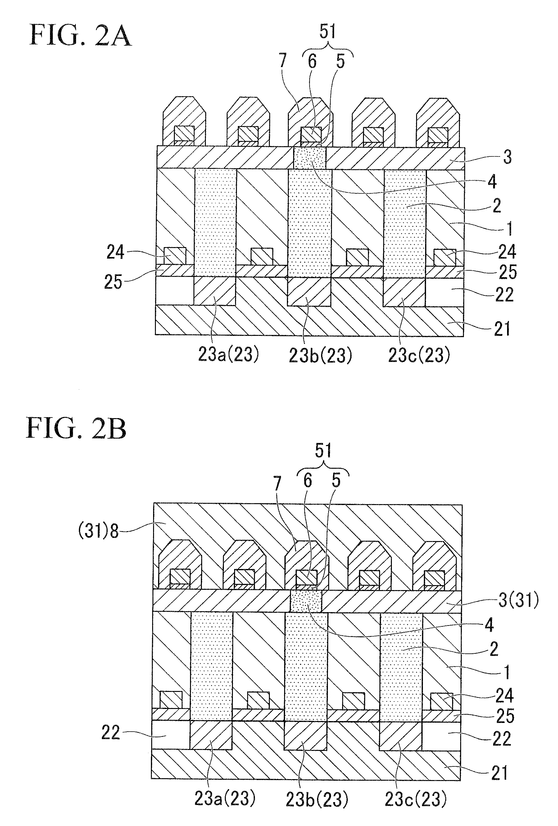
[0054]In FIG. 1A, a substrate 21 is such as a silicon substrate. An element isolation region (STI) 22 shown in FIG. 1A is formed on the substrate 21. A switching transistor is provided on the substrate 21. The switching transistor includes a gate electrode 24, a gate oxidization film 25, and an impurity dispersion layer 23 including sources 23a and 23c, and a drain 23b. A gate inte...


PUM


Abstract

A semiconductor device includes: a first interlayer insulating film; a first conductive member provided lower than the first interlayer insulating film; a contact plug that penetrates through the first interlayer insulating film, and is electrically connected to the first conductive member, the contact plug including a small-diameter part, and a large-diameter part arranged on the small-diameter part, an outer diameter of the large-diameter part being larger than an outer diameter of the small-diameter part, and the outer diameter of the large-diameter part being larger than an outer diameter of a connection face between the second conductive member and the large-diameter part; and a second conductive member that is provided on the first interlayer insulating film, and is electrically connected to the contact plug.

Description

BACKGROUND OF THE INVENTION[0001]1. Field of the Invention[0002]The present invention relates to a semiconductor device and a semiconductor device manufacturing method. The invention particularly relates to a semiconductor device and a semiconductor device manufacturing method that are suitable for application in a semiconductor device including a dynamic random access memory (DRAM) capacitor.[0003]Priority is claimed on Japanese Patent Application No. 2007-177188, filed Jul. 5, 2007, the content of which is incorporated herein by reference.[0004]2. Description of Related Art[0005]Memory cells such as a DRAM include switching transistors and capacitors. With the advancement of minute work techniques, memory cells are becoming increasingly miniaturized. This has led to a problematic decrease in the amount of charge accumulated in the capacitor. To solve this problem, the height of the capacitor is increased by utilizing a capacitor over bit-line (COB) structure and forming a cup-shap...

Claims


Application Information

Patent Timeline
IPC IPC(8): H01L27/108H01L21/8242
CPCH01L27/10855H01L27/10814H01L28/40H10B12/315H10B12/0335
Inventor NISHI, HIROO
Owner PS4 LUXCO SARL
Why Eureka
Try Eureka