RFID tag mounting circuit board

Inactive Publication Date: 2009-01-08
HITACHI LTD
View PDF5 Cites 99 Cited by
  • Summary
  • Abstract
  • Description
  • Claims
  • Application Information

AI Technical Summary

Benefits of technology

[0014]According to the present invention, it is possible to minimize decrease in the component mounting density of a printed circuit board even if

Problems solved by technology

Printed circuit board-based design is thus required, and the number of man-hours required for design increases.
In other words, lot management of components A to be used cannot be performed.
Even if an RFIC chip which is easier to individually manage than a barcode is mounted, since an ID can be generally read until after a reflow process, i.e., until the RFIC chip is soldered to a printed circuit board, it is

Method used


Image

  • RFID tag mounting circuit board
  • RFID tag mounting circuit board
  • RFID tag mounting circuit board

Examples


Example

First Embodiment

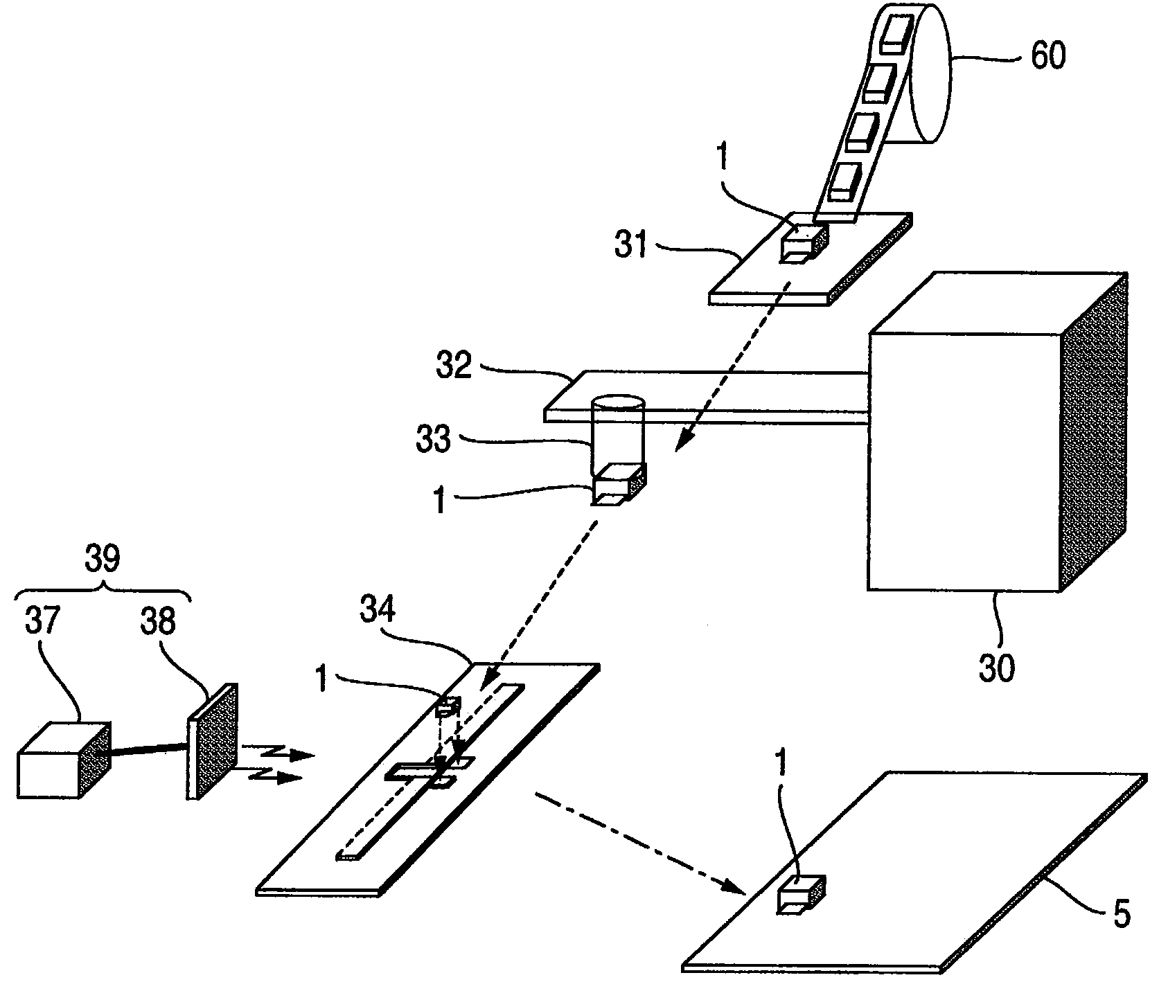
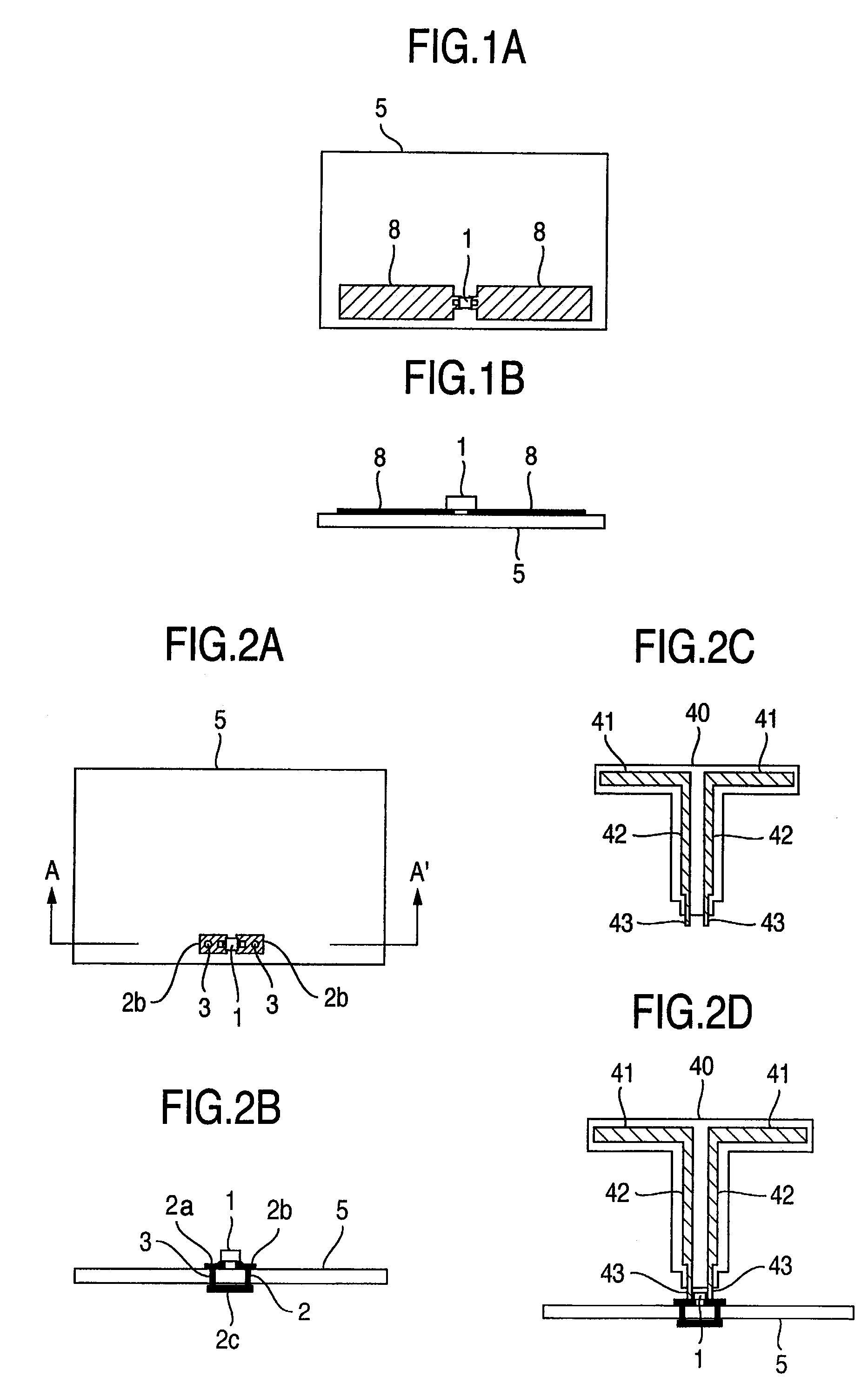
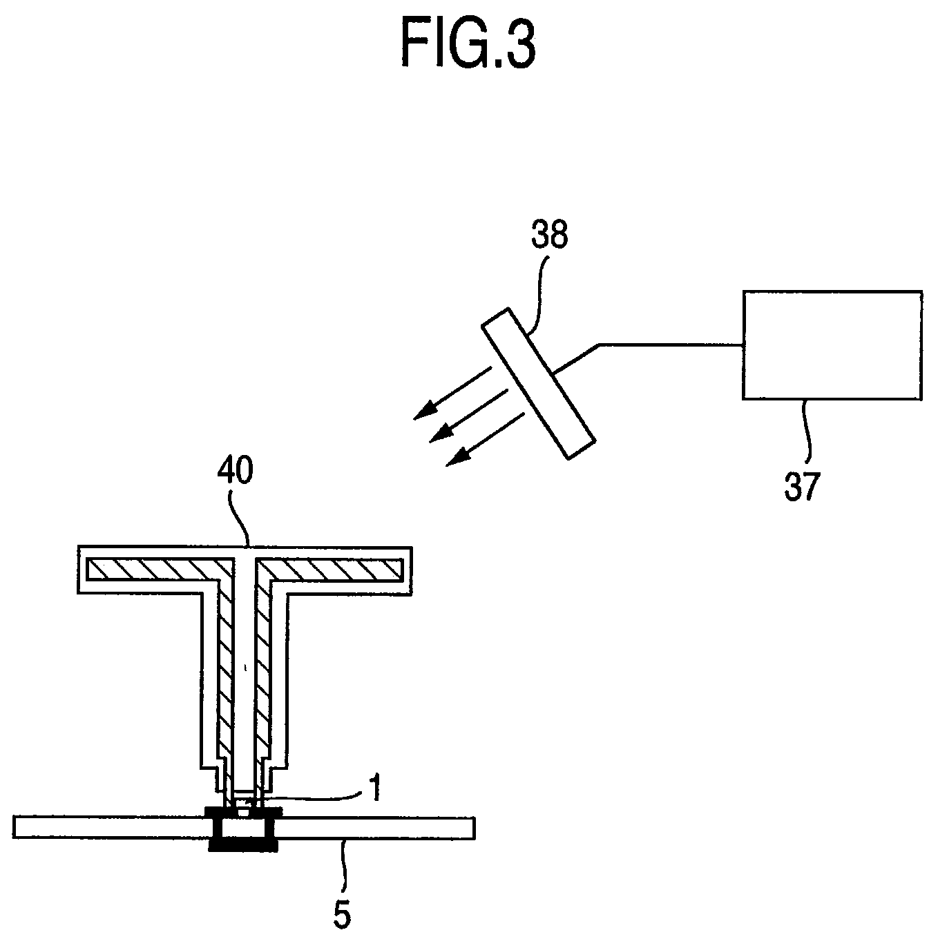
[0034]An embodiment of the present invention will be described below. FIGS. 1A and 1B are views showing a related-art configuration. As shown in FIGS. 1A and 1B, a dipole antenna with a length of ½λ is arranged on a surface of a printed circuit board in the related-art configuration. If a small printed circuit board is employed, an area occupied by an antenna used for an RFID tag increases, and the component mounting density of the printed circuit board decreases. FIG. 2A to 2D are views showing a configuration according to the present invention, which is in contrast with the related-art configuration. FIG. 2A shows a top view of the configuration in which an IC chip 1 and printed patterns 2a and 2b which connect the IC chip 1 and through holes 3 are arranged on a printed circuit board 5. FIG. 2B shows a sectional view of FIG. 2A taken along the line A-A′. FIG. 2C shows an external antenna to be connected to the IC chip 1, and FIG. 2D shows a state in which the exter...

Example

Second Embodiment

[0044]In the first embodiment, a balanced antenna, such as a dipole antenna, is used as the external antenna 40. As a second embodiment, an embodiment will be described in which an antenna of monopole type that is an unbalanced antenna is used as an external antenna 50.

[0045]FIG. 6 shows the shape of a stub formed on a printed circuit board 5. Printed patterns 2a and 2b on a surface where an IC chip 1 is mounted are the same as those in the first embodiment. A pattern on the reverse surface side is formed to have a shape like that of a printed pattern 2e. The shape is formed by connecting one end of a printed pattern 2c to a pattern larger in area than the printed pattern 2c. In many cases, specifically, a ground (ground potential) pattern is laid on the reverse surface of a printed circuit board, and the printed circuit board often has a number of large-area patterns. A pattern corresponding to the printed pattern 2c is connected to such a ground pattern.

[0046]As a...

Example

Third Embodiment

[0048]In the first and second embodiments, when reading information in the IC chip 1, the external antenna 40 or 50 is used while being connected to the IC chip 1. As a third embodiment, an embodiment will be described for a case where it is necessary to continuously or intermittently read information in an IC chip 1 for a specified period. This embodiment is designed on the assumption that the need to read information on a printed circuit board arises in processes for repair and inspection of printed circuit boards.

[0049]An external antenna 40a is clip-shaped, as shown in FIGS. 9A to 9C, and is kept up by sandwiching the IC chip 1. More specifically, the external antenna 40a is composed of a structural member 44a which forms a clip and is a molding made of a resin, such as PC (polycarbonate) or PP (polypropylene), antenna units 41a, field waveguide units 42a, and connections 43a to be connected to the IC chip 1. A springy metal, such as phosphor bronze, is used as t...


PUM


Abstract

An RFID tag mounting circuit board has a configuration in which an RFIC chip, a minimum antenna, a circuit which matches the impedance of the RFIC chip and that of the antenna are mounted on a printed circuit board. With this configuration, the area occupied by the antenna of an RFID tag is suppressed, and decrease in the component mounting density of the printed circuit board is suppressed. The RFID tag mounting circuit board is configured to be capable of managing the histories of all components on a per-printed-circuit-board basis by attaching a reading device for an RFIC chip to a chip mounter which mounts an IC chip.

Description

INCORPORATION BY REFERENCE[0001]The present application claims priority from Japanese application JP2007-174,711 filed on Jul. 3, 2007, the content of which is hereby incorporated by reference into this application.FIELD OF THE INVENTION[0002]The present invention relates to an electronic component device; more particularly, to a technique for managing a printed circuit board on which electronic components are to be mounted and components to be mounted thereon using an RFID (Radio Frequency IDentification) tag; and most particularly, to a technique for forming an RFID tag for component management on a printed circuit board.BACKGROUND OF THE INVENTION[0003]Examples of a conventional technique for managing the history of an electronic component on a printed circuit board using an RFID tag include one disclosed in JP-A-2007-66989 (Patent Document 1). Patent Document 1 discloses management of the history of an electronic component by mounting an RFID tag having an antenna and an IC chip...

Claims


Application Information

Patent Timeline
IPC IPC(8): G08B13/14
CPCG06K19/04G06K19/0726G06K19/07749G06K19/07758H01L2224/16225H05K1/0243H05K1/0266H05K2201/10098H01Q1/2225G06K19/07H01Q1/24
Inventor SAKAMA, ISAOASHIZAWA, MINORU
Owner HITACHI LTD
Why Eureka
Try Eureka